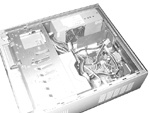
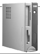
For an information processing device such as a computer, the chassis not only provides mechanical protection, but also functions as an electromagnetic shield: the computer is protected from external electromagnetic waves, so that the computer works more stably and reliably; at the same time, the computer itself can be prevented. The generated electromagnetic waves radiate outwards to avoid affecting the normal operation of other electronic devices. Therefore, the chassis design has been paid more and more attention by PC manufacturers and has become an important factor in measuring the quality of PC products. Below, we will give a brief introduction to the electromagnetic compatibility design of the computer chassis from the aspects of chassis selection, gap and opening treatment.
Box material selection
In order to improve the shielding effectiveness of the chassis, the choice of chassis materials should be considered first. Since the shielding effect of different materials is different, metal materials with high magnetic permeability and high electrical conductivity should be selected according to the efficiency of shielding and the cost ratio of raw materials.
Since the electromagnetic wave propagates in a straight line, when it propagates to the metal surface, it can not only penetrate into the thin layer of the surface of the metal body, but also produce a reflection phenomenon on the metal surface. Therefore, a chassis plate with a moderate thickness and a good smoothness should be selected: if the chassis The thickness is too thin, not only does not protect the machine, but the electromagnetic wave is easy to penetrate, the shielding effect is greatly reduced; the box is too thick, which causes unnecessary waste of raw materials; the better the surface finish of the chassis, the electromagnetic wave in the chassis The more reflective the surface is, the better the surface finish is easy to process, and the ease of processing and chemical corrosion resistance of the sheet.
Gap and opening treatment
Because there are various wiring harnesses and boards inserted and led out on the computer cabinet, such as power cables, signal cables, control cables, etc.; there are switches, indicator lights, floppy drives, optical drives, etc., and ventilation holes are also arranged for heat dissipation, so the chassis does not It may be made completely sealed, but there are more or less seams and openings - these seams and openings can cause electrical discontinuities, such as improper handling, will result in a reduction in shielding effectiveness. Therefore, in the design of the chassis, if you want to improve the electromagnetic shielding effectiveness of the product, you must make special "care" for the seams and openings.
Seam measures
Due to the unevenness of the surface of the joint of the chassis and the warpage of the thin-plate type material, a long and narrow gap will inevitably occur. According to the electromagnetic wave theory on the overall shielding effectiveness of the joint, the following measures can be taken for the chassis joint:
a. reduce the length of the gap
When the length of the slit reaches λ/4 (λ is the wavelength of the electromagnetic wave) or longer, this gap becomes a very effective radiation generator, causing a large amount of leakage of electromagnetic energy. Therefore, the open-top structure should be used as much as possible instead of the two-sided open-cover structure to reduce the total gap length. It is also possible to apply conductive material or increase the conductive gasket at the joint - since the contact surface is microscopically It is said that the joint is uneven, and the joint can only be partially contacted. Therefore, the conductive material or the conductive gasket can be applied to increase the contact surface, thereby reducing electromagnetic leakage.

Because computer products are information technology equipment, the radio disturbance characteristics should meet the relevant requirements of the "Radio Disturbance Limits and Measurement Methods for Information Technology Equipment" (GB9254-1998). In this standard, the finite value of the frequency component of the radio frequency from 150KHz to 1GHz is required. The wavelength corresponding to the highest frequency of 1GHz is 30cm, and the corresponding λ/4 is 7.5cm. Therefore, the length of the gap is required to be controlled as much as 5~7. Within centimeters. In addition, if the conditions permit, increasing the number of connecting points such as screws or reducing the spacing of the connecting points such as screws can also play the role of controlling the length of the slit.
b. Increase the depth of the gap
Increasing the depth of the gap can improve the shielding effectiveness of the chassis: from the perspective of electromagnetic leakage, increasing the overlap size at the seam is equivalent to increasing the depth of the gap, so that the electromagnetic wave passes through multiple reflections and refractions between the metal walls. The energy is consumed in a large amount, and the energy leaking from the inside of the chassis to the outside is naturally reduced accordingly (the seams of the chassis should not be arranged at the corners as much as possible, and should be placed on a large plane as much as possible). U-slit is an effective design to increase the depth of the gap.
Surface-Mount (SMT) &BGA Assembly
What is SMT PCB assembly?
SMT patch refers to the abbreviation of a series of technological processes that are processed on the basis of PCB, and PCB (Printed Circuit Board) is a printed circuit board. SMT is surface mount technology (Surface Mounted Technology) (abbreviation of Surface Mounted Technology), and it is one of the most popular technologies and processes in the PCB assembly industry.
SMT is surface mount technology (Surface Mounted Technology) (abbreviation of Surface Mounted Technology), and it is one of the most popular technologies and processes in the PCB assembly industry. Electronic circuit surface mount technology (Surface Mount Technology, SMT), called surface mount or surface mount technology. It is a kind of surface assembly components with no leads or short leads (SMC/SMD for short, chip components in Chinese) mounted on the surface of a printed circuit board (Printed Circuit Board, PCB) or the surface of other substrates. Circuit assembly technology in which reflow soldering or dip soldering is used for soldering and assembling. Under normal circumstances, the electronic products we use are designed by PCB plus various capacitors, resistors and other Electronic Components according to the designed circuit diagram, so all kinds of electrical appliances need a variety of smt patch processing techniques to process.

1. Silk screen: Its function is to leak solder paste or patch glue onto the PCB pads to prepare for the soldering of components. The equipment used is a screen printing machine (screen printing machine), located at the forefront of the SMT production line.
2. Dispensing: It is to drop the glue onto the fixed position of the PCB board, and its main function is to fix the Electronic Components on the PCB board. The equipment used is a glue dispenser, located at the forefront of the SMT production line or behind the testing equipment.
3. Mounting: Its function is to accurately mount the surface mount components to the fixed position of the PCB. The equipment used is a placement machine, located behind the screen printing machine in the SMT production line.
4. Curing: Its function is to melt the patch glue, so that the surface assembly components and the PCB board are firmly bonded together. The equipment used is a curing oven, located behind the placement machine in the SMT production line.
5. Reflow soldering: Its function is to melt the solder paste, so that the surface assembly components and the PCB board are firmly bonded together. The equipment used is a reflow oven, located behind the placement machine in the SMT production line.
6. Cleaning: Its function is to remove the solder residues such as flux that are harmful to the human body on the assembled PCB board. The equipment used is a washing machine, and the location may not be fixed, it may be online or offline.
7. Inspection: Its function is to inspect the welding quality and assembly quality of the assembled PCB board. The equipment used includes magnifying glass, microscope, online tester (ICT), flying probe tester, automatic optical inspection (AOI), X-RAY inspection system, functional tester, etc. The location can be configured in a suitable place on the production line according to the needs of the inspection.
8. Rework: Its function is to rework the PCB boards that have failed to detect faults. The tools used are soldering irons, rework stations, etc. Configured at any position in the production line.


Smt Bga Assembly,Surface Mount Technology Assembly,Wireless Charger Pcba Circuit Board,Pcba Motherboard Assembly
HAODA ELECTRONIC CO.,LIMITED , https://www.pcbhdi.com