Wafer manufacturing process 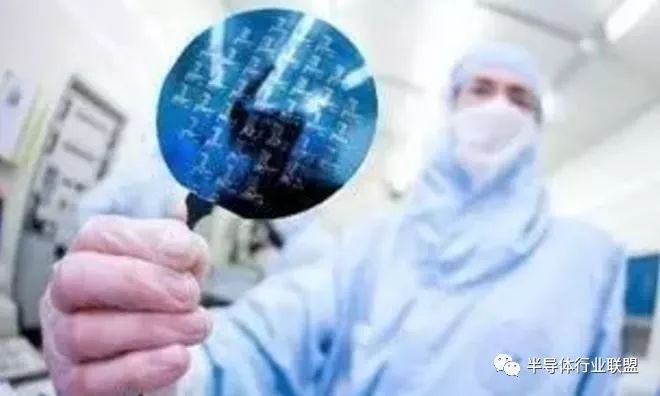
1, surface cleaning
2, primary oxidation
3. A layer of Si3N4 (Hot CVD or LPCVD) is deposited by the CVD (Chemical Vapor deposiTIon) method. (1) Normal Pressure CVD (2) Low Pressure CVD (3) Hot CVD (Hot CVD) / (thermal CVD) (4) Plasma Enhanced CVD (5) MOCVD (Metal Organic CVD) & Molecular Beam Epitaxy (6) Epitaxial Growth (LPE)
4. Coating photoresist (1) coating of photoresist (2) prebake (3) exposure (4) development (5) post bake (6) etching (etching) 7) Removal of photoresist
5. Here, the silicon nitride is removed by dry oxidation.
6. Ion implantation implants boron ions (B+3) through the SiO2 film into the substrate to form a P-type well.
7. Remove the photoresist and place it in a high temperature furnace for annealing
8. Remove the silicon nitride layer with hot phosphoric acid and dope with phosphorus (P+5) ions to form an N-type well.
9. Annealing, then removing the SiO2 layer with HF
10. A dry oxidization method produces a layer of SiO2, and then a layer of silicon nitride is deposited by LPCVD.
11. Retaining the silicon nitride layer on the lower gate isolation layer by photolithography and ion etching
12. Wet oxidation, growth of SiO2 layer without silicon nitride protection, forming an isolation region between PN
13. The hot phosphoric acid removes the silicon nitride, and then the SiO2 solution is used to remove the SiO2 at the gate isolation layer, and a better quality SiO2 film is regenerated to serve as the gate oxide layer.
14. LPCVD deposits a polysilicon layer, then applies photoresist to photolithography, as well as plasma etching techniques, gate structures, and oxidizes to form a SiO2 protective layer.
15. The surface is coated with photoresist to remove the photoresist of the P-well region and implant arsenic (As) ions to form the source and drain of the NMOS. In the same way, in the N-well region, B ions are implanted to form the source and drain of the PMOS.
16. An undoped oxide layer is deposited by PECVD to protect the component and be annealed.
17. Deposition of boron-phosphorus-doped oxide layer 18, sputtering of the first layer of metal (1) The deposition method of the film varies depending on the application, and the thickness is usually less than 1 μm. (2) EvaporaTIon DeposiTIon (3) Sputtering DeposiTIon
19. Photolithography defines a VIA hole, deposits a second layer of metal, and etches the wire structure. Then, the layer and the silicon nitride protective layer are oxidized by PECVD.
20, lithography and ion etching, to determine the PAD position
21. Finally, annealing is performed to ensure the integrity and connectivity of the entire Chip.
Wafer Manufacturing Process The manufacturing process of a chip can be divided into Wafer Fabrication, Wafer Probe, Packaging, and Initial Test and Final Test. Wait a few steps.
The wafer processing step and the wafer needle measurement step are the front end steps, and the assembly process and the test process are the back end processes.
1. Wafer processing process: The main work of this process is to make circuits and electronic components (such as transistors, capacitors, logic switches, etc.) on the wafer. The processing procedure is usually related to the product type and the technology used, but generally The steps are to properly clean the wafer, perform oxidation and chemical vapor deposition on the surface, and then perform repeated steps such as coating, exposure, development, etching, ion implantation, metal sputtering, etc., and finally complete several layers on the wafer. Circuit and component processing and fabrication.
2, wafer needle measurement process: After the previous process, the wafer is formed into a small grid, that is, the grain, in general, in order to facilitate testing, improve efficiency, the same variety is produced on the same wafer, Specifications of the product; but can also be produced according to the needs of several different varieties and specifications. Check each die with a probe
After its electrical characteristics, the unqualified crystal grains are marked, the wafer is cut, divided into individual crystal grains, and then classified according to their electrical characteristics, loaded into different trays, and unqualified crystal grains. Then give up.
3. The assembly process is to fix a single die on a plastic or ceramic chip base, and connect some lead terminals etched on the die to the pins protruding from the bottom of the base to serve as the external For the connection of the circuit board, finally cover the plastic cover and seal it with glue. Its purpose is to protect the crystal grains from mechanical scratches or high temperature damage. At this point, we have made an integrated circuit chip (that is, those black or brown that we can see in the computer, rectangular blocks with many pins or leads on both sides or four sides).
4. Test procedure: The last process of chip manufacturing is testing. It can be divided into general test and special test. The former is to test the electrical characteristics of the packaged chip under various environments, such as power consumption, running speed, Pressure resistance, etc. The tested chips are classified into different grades according to their electrical characteristics. The special test is based on the technical parameters of the customer's special needs, take some chips from the similar parameter specifications and varieties, and do specific tests to see if they can meet the special needs of customers to decide whether they need to design special for customers. chip. Products that have passed the general test are affixed with labels of specifications, models, and date of manufacture, and are packaged and shipped. Chips that fail the test are classified as downgrades or scraps depending on the parameters they reach.
Compared with traditional engineering and business education projectors, home projectors are more compact, practical and entertaining, and projection technology is more suitable for home life and entertainment scenes
Features
1. Large screen: The size of traditional LCD TVs is mostly between 40-70 inches, while home projectors can easily project 100-150 inches of screen content.
2. Diverse uses: Home projectors are mostly equipped with intelligent systems, which contain a large number of film sources. In addition, the projector can also be connected to different devices through different interfaces, such as game consoles, computers, U disks, etc. Only one machine can realize online drama, listening to songs, games, office and other functions
3. Diffuse reflection eye protection: The home projector uses the principle of diffuse reflection to form images, which is less harmful to the eyes than the LCD screen.
4. Convenient to move: The home projector is compact, light in weight, flexible in movement, and used in a variety of scenarios
Home Projectors,Production Projector,Home Theater Projectors,Bluetoth Battery Projector
Shenzhen Happybate Trading Co.,LTD , https://www.szhappybateprojectors.com