A/D conversion is a kind of operation of converting continuous analog signals into binary numbers suitable for digital processing. In a single-chip microcomputer control system, it is often necessary to convert a process signal simulated by a controlled entity into a digital quantity and send it to a single-chip microcomputer. The work is done by the A/D converter. Therefore, A/D conversion components have a wide range of applications in single chip microcomputer systems. A/D conversion is an important part of the electrical signal data acquisition system. This paper takes the self-designed ECG acquisition system as an example to introduce the specific application of the 12-bit A/D conversion chip AD574 in this system. Has a good practical application reference value.
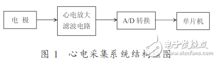
2, ECG signal acquisition systemAs an effective means of dynamic detection and analysis of human heart activity, ECG monitoring has a good application value in clinical and human quality analysis. ECG acquisition is the first step in ECG monitoring. This paper uses the general 51 MCU to control the acquisition of ECG signals. Figure 1 shows the overall block diagram of an ECG acquisition system.
The electrode is a sensitive component that obtains the ECG signal from the human body. The ECG signal is picked up by a dedicated electrode carried on the human body and sent to the amplification and filtering circuit. After amplification and filtering circuit, a clean, undistorted heart is obtained. The electric analog signal is sent to the A/D conversion circuit by the analog input terminal, and finally the high-precision A/D conversion and data storage are performed under the control of the single chip microcomputer.
The AD574 is a 12-bit successive approximation A/D converter manufactured by AnalogDevice of the United States. The internal integration consists of a conversion clock, a reference voltage source and a tri-state output latch, so that it can be directly connected to the microcomputer bus. The resolution can be set to 12 bits and the conversion time is 25μs. The external connection signals of the A/D converter include an analog input signal, a data output signal, a start conversion signal, a conversion end signal, and data reading. The connection problem of these signals should be considered when connecting the A/D converter to the system.
The AD574 is a single-ended input analog voltage. It can be input between either l0Vin and 20Vin and AGND. It can input unipolar voltage or bipolar voltage. The input analog voltage has different polarity and its input circuit is different. The AD574 requires a pulse start signal, that is, a start conversion signal is issued under the control of the CPU, and a pulse signal of a sufficient width is obtained by program control. At the end of the A/D conversion, the AD574 feedback gives the conversion end signal. The data output line of the AD574 also has a three-state output gate that can be directly connected to the system data bus. In this acquisition system, the interface circuit of AD574 and AT89S51 microcontroller is shown in Figure 2.
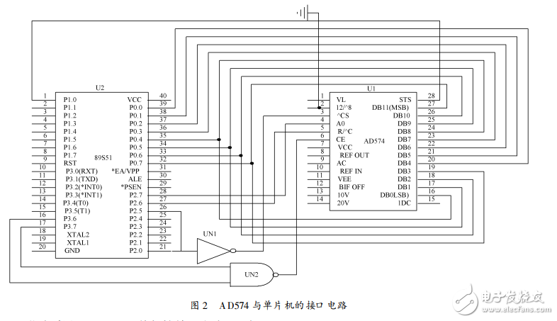
The AD574 chip uses a 0 to +10V unipolar input method. 2 feet are directly grounded, that is, 12-bit conversion is started, and the conversion result is divided into two outputs. The 3, 4, and 5 pins are respectively connected to the upper bits of the MCU address bus, P2.5, P2.4, P2.3, and the read/write signals of the MCU. After the primary NAND gate is sent to the CE foot of the AD574 as an enable signal.
The AD574 status pin STS can be connected to an external interrupt. For example, INT0 can be used to read the conversion result in interrupt mode. Of course, it can also be directly connected to the P1.0 pin of the MCU, and the conversion result can be read by query mode. Two 0.1kΨ potentiometers connected to pins 12 and 10 of AD574 are used for zero adjustment and full scale adjustment respectively. The specific adjustment method is: zero adjustment, adjust R1 to change the input analog voltage from -5V to -4.9988 V, that is, when the input voltage changes by 1/2LSB, the output digital quantity changes from 000000000000 to 000000001; full scale adjustment (ie gain adjustment), and R2 is adjusted to change the input analog voltage from +4.9988V to +5V, that is, the input voltage changes by 1/2LSB. At the time, the output digital quantity changes from 111111111110 to 111111111111.
Female Header Connector,0.80Mm Female Header Connector,2.54Mm Female Header Connector,3.96Mm Female Header Connector
Shenzhen CGE Electronic Co.,Ltd , https://www.cgeconnector.com