The energy conversion system must have energy consumption. Although 100% conversion efficiency cannot be obtained in practical applications, a high-quality power supply efficiency can reach a very high level with an efficiency close to 95%. The operating efficiency of most power ICs can be measured under specific operating conditions, and these parameters are given in the data sheet. The average manufacturer will give the actual measurement results, but we can only guarantee our own data. Figure 1 shows an example of a SMPS buck converter with a conversion efficiency of 97%, which maintains high efficiency even at light loads. What is the secret to achieve such high efficiency? We'd better start with a common understanding of SMPS losses. Switching power supplies are mostly driven by switching devices (MOSFETs and diodes), and a small fraction of the losses come from inductors and capacitors. However, if very cheap inductors and capacitors (with higher resistance) are used, the loss will increase significantly. When choosing an IC, you need to consider the architecture and internal components of the controller in order to get an efficient indicator. For example, Figure 1 uses a variety of methods to reduce losses, including: synchronous rectification, integrated low on-resistance MOSFETs inside the chip, low quiescent current and skip-pulse control modes. We will discuss the benefits of these measures in this article.
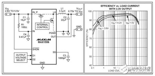
Figure 1. The buck converter integrates a low on-resistance MOSFET with synchronous rectification, and the efficiency curve is shown.
Step-down SMPS
Loss is a problem faced by any SMPS architecture. We will discuss the buck converter (buck converter) shown in Figure 2 as an example. The switching waveforms at each point are indicated for subsequent calculations.

The main function of the buck converter is to convert a higher DC input voltage into a lower DC output voltage. In order to meet this requirement, the MOSFET is turned on and off at a fixed frequency (f S ) under the control of a pulse width modulation signal (PWM). When the MOSFET is turned on, the input voltage charges the inductor and capacitors (L and C OUT ), which pass energy to the load. During this time, the inductor current rises linearly and the current loop is shown as loop 1 in Figure 2.
When the MOSFET is turned off, the input voltage is disconnected from the inductor, and the inductor and output capacitor supply the load. The inductor current drops linearly, current flows through the diode, and the current loop is shown as loop 2 in the figure. The on-time of the MOSFET is defined as the duty cycle (D) of the PWM signal. D divides each switching cycle into [D × tS] and [(1 - D) × tS], which correspond to the on-time of the MOSFET (loop 1) and the on-time of the diode (loop 2). . All SMPS topologies (buck, inverting, etc.) use this method to divide the switching cycle for voltage conversion.
For a buck converter circuit, a larger duty cycle will transfer more energy to the load and the average output voltage will increase. Conversely, when the duty cycle is low, the average output voltage will also decrease. Based on this relationship, the conversion formula for the buck type SMPS can be obtained under the following ideal conditions (regardless of the voltage drop of the diode or MOSFET):
V OUT = D × V IN
I IN = D × I OUT
It should be noted that the longer any SMPS is in a state during a switching cycle, the greater the loss it will cause in this state. For buck converters, the lower D (the lower the corresponding VOUT), the greater the losses generated by Loop 2.
1. Loss MOSFET conduction loss of switching devices
The MOSFETs and diodes in Figure 2 (and most other DC-DC converter topologies) are the main factors contributing to power consumption. The correlation loss mainly includes two parts: conduction loss and switching loss.
MOSFETs and diodes are switching elements that flow through the loop when turned on. When the device is turned on, the conduction loss is determined by the on-resistance of the MOSFET (RDS(ON)) and the forward voltage of the diode.
The conduction loss of the MOSFET (PCOND(MOSFET)) is approximately equal to the product of the on-resistance RDS(ON), the duty cycle (D), and the average current of the MOSFET when turned on (IMOSFET(AVG)).
PCOND (MOSFET) (using average current) = IMOSFET (AVG) 2 × RDS(ON) × D
The above equation gives an approximation of the MOSFET conduction loss in the SMPS, but it is only used as an estimate of the circuit loss because the power generated by the linear rise of the current is greater than the power calculated from the average current. For the “peak†current, a more accurate calculation is to integrate the square of the current waveform between the current peak and the valley (IV and IP in Figure 3) to obtain an estimate.

Figure 3. MOSFET current waveform for a typical buck converter to estimate the conduction loss of the MOSFET.
The following equation gives a more accurate way to estimate the loss, replacing the simple I2 term with the integral of the current waveform I2 between IP and IV.
PCOND(MOSFET) = [(IP3 - IV3)/3] × RDS(ON) × D
= [(IP3 - IV3)/3] × RDS(ON) × VOUT/VIN
Where, IP and IV correspond to the peak and valley values ​​of the current waveform, respectively, as shown in Figure 3. The MOSFET current rises linearly from IV to IP, for example: if IV is 0.25A, IP is 1.75A, RDS(ON) is 0.1Ω, VOUT is VIN/2 (D = 0.5), based on average current (1A) for:
PCOND (MOSFET) (using average current) = 12 × 0.1 × 0.5 = 0.050W
Use waveform integration for more accurate calculations:
PCOND (MOSFET) (calculated using current waveform integration) = [(1.753 - 0.253)/3] × 0.1 × 0.5 = 0.089W
Or approximately 78%, higher than the result calculated from the average current. For current waveforms with relatively small peaks, the difference between the two calculation results is small, and the average current calculation can meet the requirements.
2, diode conduction loss
The conduction loss of the MOSFET is proportional to R DS(ON) , and the conduction loss of the diode is highly dependent on the forward voltage (VF). Diodes are typically more lossy than MOSFETs, and diode losses are proportional to forward current, VF, and on-time. Since the diode is turned on when the MOSFET is turned off, the conduction loss of the diode (P COND(DIODE) ) is approximately:
PCOND(DIODE) = IDIODE(ON) × VF × (1 - D)
Where IDIODE(ON) is the average current during diode turn-on. As shown in Figure 2, the average current during diode turn-on is IOUT, so for a buck converter, PCOND(DIODE) can be estimated as follows:
PCOND(DIODE) = IOUT × VF × (1 - VOUT/VIN)
Unlike the MOSFET power calculation, the average current is used to get a more accurate power calculation because the diode loss is proportional to I, not I2.
Obviously, the longer the on-time of the MOSFET or diode, the greater the conduction loss. For a buck converter, the lower the output voltage, the greater the power consumed by the diode because the longer it is in the on state.
3, switching dynamic loss
Since switching losses are caused by non-ideal states of the switches, it is difficult to estimate the switching losses of the MOSFETs and diodes. It takes some time for the device to go from fully on to fully off or from fully off to fully on, producing power during this process. loss. The drain-to-source voltage (VDS) and drain-source current (IDS) of the MOSFET shown in Figure 4 are a good illustration of the switching losses of the MOSFET during the transition. As can be seen from the upper half of the waveform, tSW(ON) and The voltage and current are transient during tSW(OFF), and the capacitance of the MOSFET is charged and discharged.
As shown in Figure 4, the full load current (ID) flows through the MOSFET before the VDS falls to the final conduction state (= ID × RDS(ON)). Conversely, when turned off, VDS gradually rises to the final value of the off state before the MOSFET current drops to zero. During the switching process, the overlap of voltage and current is the source of switching losses, as can be clearly seen in Figure 4.
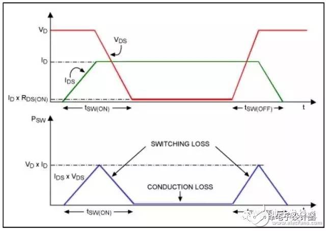
Figure 4. Switching losses occur during the transition between MOSFET on and off
The switching loss increases as the SMPS frequency increases. It is easy to understand that as the switching frequency increases (the period is shortened), the proportion of the switching transition time increases, thereby increasing the switching loss. During switching, the switching time is one-twentieth of the duty cycle. The effect on efficiency is much less than the case where the switching time is one tenth of the duty cycle. Since switching losses have a large relationship with frequency, switching losses will become the main loss factor when operating at high frequencies. The switching loss of the MOSFET (PSW(MOSFET)) can be estimated according to the triangular wave shown in Figure 3. The formula is as follows:
PSW (MOSFET) = 0.5 × VD × ID × (tSW(ON) + tSW(OFF)) × fS
Where VD is the drain-to-source voltage during MOSFET turn-off, ID is the channel current during MOSFET turn-on, and tSW(ON) and tSW(OFF) are turn-on and turn-off times. For buck circuit conversion, VIN is the voltage at which the MOSFET is turned off, and the current when turned on is IOUT.
To verify the switching losses and conduction losses of the MOSFET, Figure 5 shows typical waveforms for integrating high-side MOSFETs in a buck converter: VDS and IDS. The circuit parameters are: VIN = 10V, VOUT = 3.3V, IOUT = 500mA, RDS(ON) = 0.1Ω, fS = 1MHz, and switching transient time (tON + tOFF) totaling 38ns.
As can be seen in Figure 5, the switching changes are not instantaneous, and the overlap of the current and voltage waveforms results in power loss. When the MOSFET is "on" (Figure 2), the current flowing through the inductor, IDS, rises linearly, and the switching loss is greater when turned off than the conduction edge.
Using the above approximate calculation method, the average loss of the MOSFET can be calculated by:
PT (MOSFET) = PCOND (MOSFET) + PSW (MOSFET)
= [(I13 - I03)/3] × RDS(ON) × VOUT/VIN + 0.5 × VIN × IOUT × (tSW(ON) + tSW(OFF)) × fS
= [(13 - 03)/3] × 0.1 × 3.3/10 + 0.5 × 10 × 0.5 × (38 × 10-9) × 1 × 106
= 0.011 + 0.095 = 106mW
This result is close to the 117.4mW measured by the curve in Figure 5. Note that in this case, fS is high enough and PSW (MOSFET) is the main factor of power consumption.
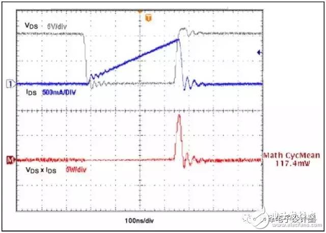
Figure 5. Typical switching cycle for a high-side MOSFET of a buck converter with 10V input and 3.3V output (500mA output current). The switching frequency is 1MHz and the switching transition time is 38ns.
Like the MOSFET, the diode also has switching losses. This loss is largely dependent on the diode's reverse recovery time (tRR), which occurs during the diode's transition from forward conduction to reverse cutoff.
When a reverse voltage is applied across the diode, the accumulated charge generated by the forward conduction current on the diode needs to be released, producing a reverse current spike (IRR(PEAK)) with a polarity opposite to the forward conduction current, resulting in V × I power loss, because the reverse voltage and reverse current exist simultaneously in the diode during the reverse recovery period. Figure 6 shows a schematic diagram of the PN junction of the diode during reverse recovery.
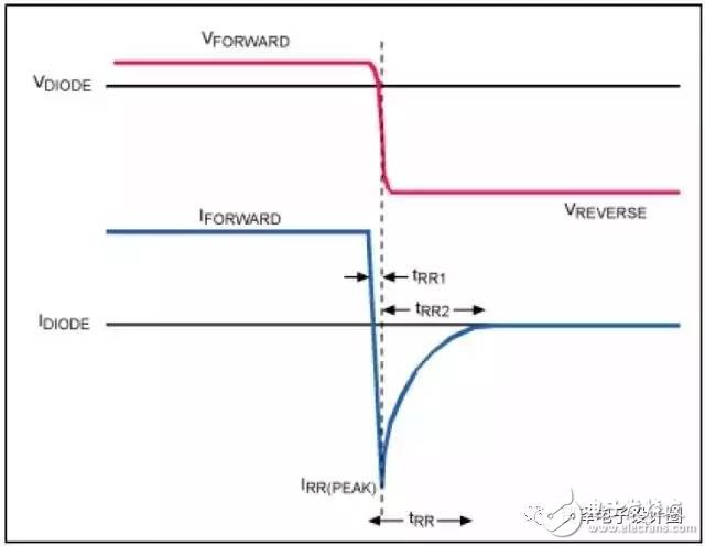
Figure 6. When the diode junction is reverse biased, the accumulated charge during forward conduction is required to generate a peak current (IRR(PEAK)).
Knowing the reverse recovery characteristics of the diode, the diode's switching loss (PSW(DIODE)) can be estimated from:
PSW(DIODE) = 0.5 × VREVERSE × IRR(PEAK) × tRR2 × fS
Among them, VREVERSE is the reverse bias voltage of the diode, IRR (PEAK) is the peak value of the reverse recovery current, and tRR2 is the time from the reverse current peak IRR to the recovery current is positive. For buck circuits, when the MOSFET is turned on, VIN is the reverse bias voltage of the diode when the MOSFET is turned on.
To verify the diode loss calculation formula, Figure 7 shows the switching waveform of the PN junction in a typical buck converter, VIN = 10V, VOUT = 3.3V, measured IRR(PEAK) = 250mA, IOUT = 500mA, fS = 1MHz, tRR2 = 28ns, VF = 0.9V. Use these values ​​to get:
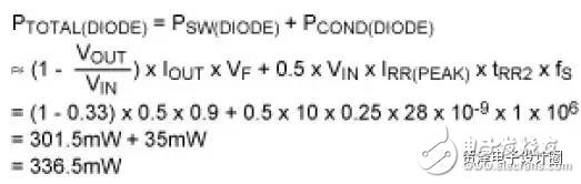
This result is close to the measurement result of 358.7 mW shown in Fig. 7. Considering the large VF and longer diode turn-on period, the t RR time is very short and the switching loss (P SW(DIODE) ) dominates the diode losses.
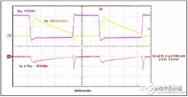
Figure 7. The switching waveform of the PN junction switching diode in a buck converter, from a 10V input to a 3.3V output, with an output current of 500mA. Other parameters include: fS at 1MHz, 28ns for tRR2, and VF = 0.9V.
Improve efficiency
Based on the above discussion, what ways can you reduce the switching loss of the power supply? The direct path is to select a low on-resistance RDS(ON), a fast-switching MOSFET, a low-conduction voltage drop VF, and a diode that can be quickly recovered.
There are several factors that directly affect the on-resistance of the MOSFET. Usually, the chip size and drain-to-source breakdown voltage (VBR(DSS)) are increased. By increasing the semiconductor material in the device, it helps to reduce the on-resistance RDS(ON). . On the other hand, larger MOSFETs increase switching losses. Therefore, while large MOSFETs reduce RDS(ON), they also cause efficiency problems that small devices can avoid. As the die temperature increases, the MOSFET's on-resistance increases accordingly. The junction temperature must be kept low so that the on-resistance RDS(ON) is not excessive. The on-resistance RDS(ON) is inversely proportional to the gate-source bias voltage. Therefore, it is recommended to use a sufficiently large gate voltage to reduce the RDS(ON) loss, but this will also increase the gate drive loss and balance the RDS. (ON) benefits and increases gate drive defects. The switching losses of MOSFETs are related to device capacitance. Larger capacitors require longer charging times, making switch switching slower and consuming more energy. Miller capacitance in MOSFET data is generally defined as the reverse transfer capacitance (CRSS) or the gate - drain capacitance (CGD), during switching to play a decisive role switching time. The charge charge of the Miller capacitor is represented by QGD. To quickly switch the MOSFET, the Miller capacitance is as low as possible. In general, the capacitance of the MOSFET is inversely proportional to the chip size, so switching losses and conduction losses must be compromised, and the switching frequency of the circuit must be carefully chosen. For diodes, the turn-on voltage drop must be reduced to reduce the resulting losses. For small, low-voltage silicon diodes, the turn-on voltage drop is typically between 0.7V and 1.5V. Diode size, process, and withstand voltage levels all affect turn-on voltage drop and reverse recovery time. Large size diodes typically have higher VF and tRR, which can result in larger losses. Switching diodes are generally divided into "high speed", "very high speed" and "super high speed" diodes, and the reverse recovery time decreases as the speed increases. The Fast Recovery Diode has a tRR of a few hundred nanoseconds, while the ultrafast fast recovery diode has a tRR of tens of nanoseconds. In low-power applications, one option to replace the fast recovery diode is the Schottky diode. The recovery time of this diode is almost negligible, and the reverse recovery voltage VF is only half that of the fast recovery diode (0.4V to 1V), but Schottky diodes are rated for voltages and currents that are much lower than fast recovery diodes and cannot be used in high voltage or high power applications. In addition, Schottky diodes have higher reverse leakage currents than silicon diodes, but these factors do not limit its use in many power supplies. However, in some low voltage applications, even with Schottky diodes with lower voltage drops, the resulting conduction losses are unacceptable. For example, in a circuit with 1.5V output, even with a Schottky diode with a 0.5V turn-on voltage drop of VF, 33% of the output voltage is lost when the diode is turned on! To solve this problem, a MOSFET with a low on-resistance RDS(ON) can be selected to implement a synchronous control architecture. Replace the diode with a MOSFET (compare Figure 1 and Figure 2), which works in sync with the main MOSFET of the power supply, so only one turn-on is guaranteed during the alternate switching process. The turned-on diode is replaced by a turn-on MOSFET, and the diode's high turn-on voltage drop, VF, is converted to the MOSFET's low turn-on voltage drop (MOSFET RDS(ON) × I), effectively reducing the conduction losses of the diode. Of course, synchronous rectification only reduces the voltage drop of the MOSFET compared to the diode. On the other hand, the power consumption of driving the synchronous rectification MOSFET cannot be ignored. IC Data Sheets Two important factors (MOSFETs and diodes) that affect the efficiency of switching power supplies are discussed above. Looking back at the step-down circuit shown in Figure 1, the main factors affecting the efficiency of the controller IC can be obtained from the data sheet. First, the switching elements are integrated inside the IC to save space and reduce parasitic losses. Second, with a low on-resistance RDS(ON) MOSFET, the NMOS and PMOS on-resistance can be 0.27Ω (typ) and 0.19Ω (typ) in a small integrated step-down IC such as the MAX1556. . Finally, the synchronous rectification circuit used. For a 500mA load, a 50% duty cycle switching circuit can reduce the loss of the low side switch (or diode) from 225mW (assuming a diode drop of 1V) to 34mW. Reasonable choice of SMPS IC Reasonable selection of the packaging and control architecture of the SMPS IC, and reasonable design, can effectively improve the conversion efficiency.
4, integrated power switch
The integration of the power switch into the IC eliminates the need for cumbersome MOSFET or diode selection and makes the circuit more compact, which can improve efficiency to some extent by reducing line losses and parasitics. MOSFETs, diodes (or synchronous rectification MOSFETs) can be integrated into the chip, depending on power level and voltage limits. Another benefit of integrating the switch inside the chip is that the size of the gate drive circuit has been optimized for on-chip MOSFETs, eliminating the need to waste time on unknown discrete MOSFETs.
Quiescent Current
Battery-powered devices pay special attention to the quiescent current (IQ) in the IC specification, which is the current required to maintain the circuit operation. Under heavy load conditions (more than ten or hundreds of quiescent current IQ), the effect of IQ on efficiency is not obvious, because the load current is much larger than IQ, and as the load current decreases, the efficiency tends to decrease because IQ corresponds to The ratio of power to total power increases. This is especially important for applications that are in sleep mode or other low-power modes most of the time. Many consumer products need to maintain keyboard scans or other functions even when they are in the "off" state. Very low IQ power supply.
Power architecture improves efficiency
The control architecture of the SMPS is one of the key factors affecting the efficiency of the switching power supply. This has been discussed in the synchronous rectification architecture. Since the MOSFET with low on-resistance replaces the switching diode with higher power consumption, the efficiency index can be effectively improved.
Another important control architecture is designed for light duty operation or a wide range of loads, namely the skip mode, also known as pulse frequency modulation (PFM). Unlike pure PWM switching operation (which uses a fixed switching frequency for both heavy and light loads), the converter operates in a skipping switching cycle in skip mode, saving unnecessary switching and increasing efficiency.
In the skip mode, the inductor discharges for a long period of time, transferring energy from the inductor to the load to maintain the output voltage. Of course, as the load sinks current, the output voltage will also drop. When the voltage drops to the set threshold, a new switching cycle is initiated to charge the inductor and replenish the output voltage.
It should be noted that the skip mode produces load-dependent output noise that is difficult to filter due to its distribution at different frequencies (different from fixed-frequency PWM control architectures).
Advanced SMPS ICs take advantage of both: a constant PWM frequency for heavy loads and a skip mode for light loads to increase efficiency. The IC shown in Figure 1 provides this mode of operation.
When the load is increased to a higher rms value, the skip pulse waveform will be converted to a fixed PWM, and the noise is easily filtered out under nominal load. Throughout the entire operating range, the device selects the skip mode and PWM mode as needed to maintain the highest overall efficiency (Figure 8).
The efficiency curves shown by curves D, E, and F in Figure 8 are less efficient at light loads in fixed PWM mode, but provide high conversion efficiency (up to 98%) at heavy loads. If the setting is to maintain a fixed PWM operating mode under light load, the IC will not change the operating mode according to the load. In this case, the ripple can be kept at a fixed frequency, but a certain amount of power is wasted. At heavy loads, the extra power required to maintain PWM switching operation is small, far below the output power. On the other hand, the efficiency curve (A, B, C in Figure 8) of the skip pulse "idle" mode can be kept at a high level at light loads because the switch is only turned on when the load requires it. For a 7V input curve, more than 60% efficiency can be achieved in idle mode with 1mA load.
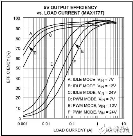
Figure 8. Efficiency curve of the buck converter in PWM and idle (jump pulse) mode. Note: At light load, the efficiency in idle mode is higher than PWM mode.
Optimize SMPS
Switching power supplies are widely used for their high efficiency specifications, but their efficiency is still limited by some inherent losses of the SMPS circuit. When designing a switching power supply, it is necessary to carefully study the source of the SMPS loss, and select the SMPS IC reasonably to take full advantage of the advantages of the device, in order to obtain an efficient SMPS while maintaining the lowest possible circuit cost or even without increasing the circuit cost. A comprehensive choice is needed.
5, passive component loss
We have learned that MOSFETs and diodes can cause SMPS losses. The use of high-quality switching devices can greatly improve efficiency, but they are not the only components that can optimize power efficiency.
Figure 1 details the basic circuit of a typical buck converter IC. Integrated two synchronous rectification MOSFETs, low RDS(ON) MOSFETs, are highly efficient. In this circuit, the switching element integrated in the IC, the pre-selected element device for specific applications. However, to further increase efficiency, designers also need to focus on passive components—external inductors and capacitors—to understand their impact on power consumption.
6, inductive power consumption resistive loss
Inductor power consumption includes two basic factors: coil loss and core loss. The coil loss is attributed to the DC resistance (DCR) of the coil, which is attributed to the magnetic characteristics of the inductor.
DCR is defined as the following resistance formula:

Where Ï is the resistivity of the coil material, l is the length of the coil, and A is the cross-sectional area of ​​the coil.
The DCR will increase as the length of the coil increases and decrease as the cross-sectional area of ​​the coil increases. This principle can be used to determine the standard inductance and determine the different inductance values ​​and sizes required. For a fixed inductance value, when the inductor size is small, the cross-sectional area of ​​the coil must be reduced in order to maintain the same number of turns, thus causing the DCR to increase; for a given inductor size, the small inductance value usually corresponds to a small DCR because A smaller number of coils reduces the length of the coil, and a wire with a larger diameter can be used.
Knowing the DCR and the average inductor current (depending on the SMPS topology), the resistance loss (PL(DCR)) of the inductor can be estimated using the following equation:
PL(DCR) = LAVG2× DCR
Here, IL (AVG) is the average DC current flowing through the inductor. For a buck converter, the average inductor current is the DC output current. Although the size of the DCR directly affects the power dissipation of the inductor resistance, which is proportional to the square of the inductor current, it is necessary to reduce the DCR.
In addition, it should be noted that when calculating the PL (DCR) (such as the above formula) using the average current of the inductor, the result is slightly lower than the actual loss because the actual inductor current is a triangular wave. In the calculation of MOSFET conduction loss described earlier in this paper, more accurate results can be obtained by integrating the waveform of the inductor current. more acurrate. Of course, the more complicated calculation formula is as follows:
PL(DCR) = (IP3 - IV3)/3 × DCR
Where IP and IV are the peak and valley values ​​of the inductor current waveform.
7, core loss
Core loss is not as easy to estimate as conduction losses and is difficult to estimate. It consists of hysteresis and eddy current losses, which directly affect the alternating flux of the core. In SMPS, although the average DC current flows through the inductor, the ripple current generated by the change in the switching voltage of the inductor causes a periodic magnetic flux change of the core.
The hysteresis loss is derived from the power dissipated by the rearrangement of the core dipoles in each AC cycle. It can be regarded as the “friction†loss caused by the friction of the dipoles when the polarity of the magnetic field changes, proportional to the frequency and magnetic Through density.
In contrast, eddy current losses are introduced by time-varying magnetic fluxes in the core. It is known from Faraday's law that alternating magnetic flux produces alternating voltage. Therefore, this alternating voltage produces a local current that produces I2R losses in the core resistance.
The core material has a great influence on the core loss. The commonly used inductor in the SMPS power supply is the iron powder core. The iron-nickel-molybdenum magnetic powder core (MPP) has the lowest loss, the iron powder core has the lowest cost, but the core loss is large.
Core loss can be estimated by calculating the maximum amount of change in core flux density (B), and then looking at the flux density and core loss (and frequency) graphs provided by the inductor or core manufacturer. The peak flux density can be calculated in several ways, and the formula can be found in the core loss curve in the inductor data sheet.
Accordingly, if the core area and the number of coils are known, the peak flux can be estimated using the following equation:
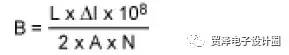
Here, B is the peak magnetic flux density (Gauss), L is the coil inductance (Heng), ΔI is the peak-to-peak value of the inductor ripple current (amperes), A is the core cross-sectional area (cm2), and N is the number of turns of the coil.
With the popularity of the Internet, it is easy to download data from the Internet and search for device information. Some manufacturers provide interactive inductive power consumption calculation software to help designers estimate power consumption. Use these tools to quickly and accurately estimate the power loss in your application circuit. For example, Coilcraft provides an online inductor core loss and copper loss calculation formula that simply inputs some data to get the core loss and copper loss of the selected inductor.
8, capacitance loss
In contrast to the ideal capacitive model, the actual physical characteristics of the capacitive element result in several losses. Capacitors act primarily in the SMPS circuit to regulate and filter out input/output noise (Figure 1). These losses in the capacitor reduce the efficiency of the switching power supply. These losses are mainly manifested in three aspects: equivalent series resistance loss, leakage current loss and dielectric loss.
The resistive losses of the capacitor are obvious. Since current flows into and out of the capacitor during each switching cycle, the inherent resistance of the capacitor (RC) will cause some power dissipation. Leakage current loss is the power loss due to the resistance (RL) of the capacitor insulation material causing a small current to flow through the capacitor. The dielectric loss is more complicated. Due to the application of an alternating voltage across the capacitor, the electric field of the capacitor changes, causing power loss due to polarization of the dielectric molecules.

Figure 9. The capacitance loss model is generally simplified to an equivalent series resistance (ESR)
All three losses are reflected in the typical loss model of the capacitor (left part of Figure 9), with resistors representing each loss. The power of each loss associated with capacitive energy storage is expressed in terms of power dissipation factor (DF), or loss tangent (δ). The DF of each loss can be obtained by the ratio of the real and imaginary parts of the capacitive impedance, and each loss can be inserted into the model separately.
To simplify the loss model, the contact resistance loss, leakage current loss, and dielectric loss concentration in Figure 9 are an equivalent series resistance (ESR). ESR is defined as the portion of the capacitive impedance that consumes active power.
When estimating the capacitive impedance model and calculating the ESR (the real part of the result), ESR is a function of frequency. This correlation can be demonstrated in the simplified ESR equation below:

Where DFR, DFL, and DFD are the power dissipation factors for contact resistance, leakage current, and dielectric loss.
Using this equation, we can observe that as the signal frequency increases, both leakage current loss and dielectric loss decrease until the contact resistance loss dominates from a higher frequency point. Above this frequency point (which is not included in the equation), the ESR tends to increase due to the skin effect of the high-frequency alternating current.
Many capacitor manufacturers offer ESR plots that show the relationship between ESR and frequency. For example, TDK provides an ESR curve for most of its capacitor products. Refer to these graphs corresponding to the switching frequency to get the ESR value.
However, if there is no ESR plot, the ESR can be roughly estimated from the DF specification in the capacitance data sheet. DF is the overall DF of the capacitor (including all losses), and the ESR can also be estimated as follows:

Either way, to get the ESR value, intuition tells us that high ESR will reduce the efficiency of the switching power supply, since the input and output capacitors are charged and discharged through the ESR every switching cycle. This results in an I2 x RESR power loss. This loss (PCAP (ESR)) can be calculated as follows:
PCAP(ESR) = ICAP(RMS)2 × RESR
Where, ICAP (RMS) is the rms RMS of the alternating current flowing through the capacitor. For the output capacitance of the buck circuit, the effective value RMS of the inductor ripple current can be used. The calculation of the RMS current of the input filter capacitor is complicated, and a reasonable estimate can be obtained according to the following formula:
ICIN(RMS) = IOUT/VIN × [VOUT (VIN - VOUT)]1/2
Obviously, to reduce capacitive power loss, a low ESR capacitor should be chosen to help the SMPS supply reduce ripple current. ESR is the main cause of output voltage ripple, so choosing a low ESR capacitor not only improves efficiency, but also other benefits.
In general, capacitors of different types of dielectrics have different ESR ratings. Aluminum electrolytic and tantalum capacitors have higher ESR values ​​than ceramic capacitors for specific capacities and voltage ratings. Polyester and polypropylene capacitors have an ESR between them, but these capacitors are large and rarely used in SMPS.
For a given type of capacitor, a larger capacity, lower fS can provide a lower ESR. Larger capacitors also typically reduce ESR, but electrolytic capacitors result in larger equivalent series inductance. Ceramic capacitors are considered a good compromise. In addition, the lower capacitor voltage rating also helps to reduce ESR under certain capacitance values.
China Phase Control Stud Thyristor,Stud Version Phase Control Thyristor supplier & manufacturer, offer low price, high quality Dc Power Encapsulation Thyristors,High Power Drives Thyristor Power Control, etc.
The output voltage of thyristor phase-controlled rectifier circuit can be regulated in a large range and has a small fluctuation, which has an impact on the electrical performance of ac power and devices.
Phase Control Stud Thyristor,Stud Version Phase Control Thyristor,Dc Power Encapsulation Thyristors,High Power Drives Thyristor Power Control
YANGZHOU POSITIONING TECH CO., LTD. , https://www.pst-thyristor.com