Layout is one of the most basic job skills for PCB design engineers. The quality of the traces will directly affect the performance of the entire system. Most of the high-speed design theories will eventually be implemented and verified through Layout. It can be seen that wiring is critical in high-speed PCB design. The following will analyze the rationality of some situations that may be encountered in the actual cabling, and give some comparatively optimized cabling strategies.
Mainly from the right-angle alignment, differential alignment, serpentine and other three aspects to elaborate.
1. Right angle alignment
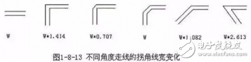
Right-angle alignment is generally a situation that PCB wiring needs to avoid as much as possible, and it is almost one of the standards to measure the quality of the wiring. How much influence does the right-angle wiring have on signal transmission? In principle, a right-angled trace will cause the linewidth of the transmission line to change, resulting in an impedance discontinuity. In fact, not only the right-angle traces, but also the angles of sharp angles and acute angles may cause impedance changes.
The effect of right-angle alignment on the signal is mainly reflected in three aspects:
One is that the corner can be equivalent to the capacitive load on the transmission line and slow down the rise time;
Second, the impedance discontinuity will cause signal reflection;
The third is the EMI produced by the right-angle tip.
The parasitic capacitance due to the right angle of the transmission line can be calculated by the following empirical formula:
C=61W(Er)1/2/Z0
In the above equation, C refers to the equivalent capacitance of the corner (unit: pF), W refers to the width of the trace (unit: inch), εr refers to the dielectric constant of the dielectric, and Z0 is the characteristic impedance of the transmission line. For example, for a 4Mils 50-ohm transmission line (εr of 4.3), a right-angle brings about 0.0101pF, which can be used to estimate the rise time variation caused by this:
T10-90%=2.2*C*Z0/2=2.2*0.0101*50/2=0.556ps
It can be seen from the calculation that the capacitive effect brought by the right-angle trace is extremely small.
As the line width of the right angle trace increases, the impedance at this point will decrease, and a certain signal reflection phenomenon will occur. We can calculate the equivalent impedance after the line width is increased according to the impedance calculation formula mentioned in the transmission line section, and then Calculate the reflection coefficient according to an empirical formula:
Ï=(Zs-Z0)/(Zs+Z0)
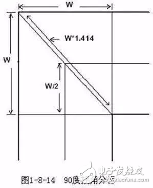
The impedance change caused by a generally right-angled trace is between 7% and 20%, and the maximum reflection coefficient is about 0.1. Moreover, as can be seen from the figure below, the impedance of the transmission line changes to the minimum during the W/2 line time, and then returns to the normal impedance after W/2 time, and the entire impedance change takes a very short time, often at 10ps. Internally, such rapid and minor changes are almost negligible for general signal transmission.
Many people have such an understanding of right-angle alignment that the tip is easy to emit or receive electromagnetic waves, resulting in EMI, which has become one of the reasons why many people think that they can not run at right angles. However, the results of many actual tests show that right-angle traces do not produce significant EMI compared to straight lines. Perhaps the current instrument performance and test level limit the accuracy of the test, but it at least illustrates a problem that the radiation of the right-angle trace is less than the measurement error of the instrument itself.
In general, right-angle alignments are not as frightening as they are. At least in applications below GHz, any effects such as capacitance, reflection, and EMI that are produced in the TDR test can hardly be reflected. High-speed PCB design engineers should focus on layout, power/ground design, and trace design. Other aspects such as vias. Of course, although the influence of right-angle alignment is not very serious, it does not mean that we can all follow the right-angled line. Attention to detail is an essential quality for every outstanding engineer. Moreover, with the rapid development of digital circuits, PCB The frequency of signals processed by engineers will also continue to increase, and in the area of ​​RF design above 10 GHz, these small right angles may become the focus of high-speed problems.
2. Differential traces
The differential signal (DifferenTIalSignal) is more and more widely used in high-speed circuit design. The most critical signal in the circuit is always designed with a differential structure. What other way is it so popular? How can we ensure good performance in PCB design? With these two questions, we will discuss the next section.
What is a differential signal? In layman's terms, the driver sends two equal-valued, inverted signals. The receiver determines whether the logical state is "0" or "1" by comparing the difference between these two voltages. The pair of traces carrying the differential signal is called differential trace.
The most obvious advantages of differential signals compared to common single-ended signal traces are reflected in the following three aspects:
a. Strong anti-interference ability, because the coupling between two differential traces is very good, when there is noise interference in the outside world, it is almost simultaneously coupled to two lines, and the receiver only cares about the difference between the two signals. So the external common mode noise can be completely canceled.
b. Effectively suppresses EMI, the same reason, because the polarities of the two signals are reversed, the electromagnetic field they radiate to each other can cancel each other out, the closer the coupling is, the less electromagnetic energy is discharged to the outside world.
c. accurate timing positioning, because the differential signal switching is located at the intersection of the two signals, rather than the ordinary single-ended signal depends on the level of the two threshold voltage to determine, and therefore affected by the process, the temperature is small, can reduce the timing error At the same time, it is also more suitable for low-amplitude signal circuits. The current low-voltage differential signaling (LVDS) refers to this small-amplitude differential signal technique.
For PCB engineers, the most important thing is to ensure that these advantages of differential routing can be fully utilized in actual wiring. Maybe as long as people who come into contact with Layout understand the general requirements of differential routing, it is "equal length, isometric." The equal length is to ensure that the two differential signals keep the opposite polarity at all times, reducing the common mode component; the equal distance is mainly to ensure the consistency of the two differential impedances and reduce the reflection. "As close as possible to principle" is sometimes one of the requirements of differential routing. However, all of these rules are not intended to be applied mechanically. Many engineers do not seem to understand the nature of high-speed differential signaling.
The following focuses on some common misunderstandings in PCB differential signal design.
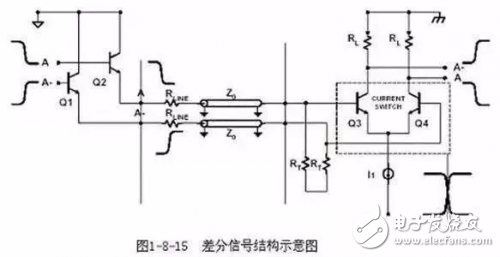
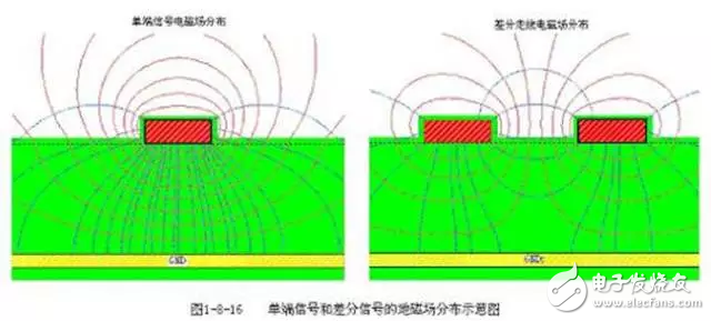
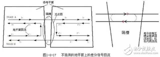
Myth #1: Think of the differential signal as not requiring a ground plane as a return path, or thinking that the differential traces provide a return path for each other. The reason for this misunderstanding is that it is confused by superficial phenomena, or the understanding of the mechanism of high-speed signal transmission is not deep enough. From the structure of the receiving end in Figure 1-8-15, it can be seen that the emitter currents of transistors Q3 and Q4 are equal and reversed. Their currents at the ground just cancel each other out (I1=0), so the differential circuit is Similar ground shots and other noise signals that may be present on the power and ground planes are insensitive. The partial return offset of the ground plane does not mean that the differential circuit does not use the reference plane as the signal return path. In fact, in the signal reflow analysis, the mechanism of the differential trace and the common single-ended trace is the same, that is, the high frequency signal is always The most important difference is that the differential line carries out the re-flow along the smallest loop of the inductor. In addition to the coupling to the ground, the differential line is also coupled with each other. Which type of coupling is strong is the main return path. Figure 1-8-16 shows the geomagnetic field distribution of single-ended signals and differential signals.
In the PCB circuit design, the coupling between the differential traces is generally small, often only accounting for 10% to 20% of the coupling degree, and more still is the coupling to the ground, so the main return path of differential traces still exists in the ground plane . When there is a discontinuity in the local plane, there is no reference plane area, and the coupling between differential traces will provide the main return path, as shown in Figure 1-8-17. Although the influence of the discontinuity of the reference plane on the differential traces is not serious for ordinary single-ended traces, it will still reduce the quality of the differential signal and increase the EMI, which should be avoided as much as possible. Some designers believe that the reference plane below the differential trace can be removed to suppress some of the common-mode signals in the differential transmission. However, in theory, this approach is undesirable, and how is the impedance controlled? Not providing a common-mode signal ground impedance loop will inevitably cause EMI radiation. This is more harm than good.
Myth #2: I think it's more important to keep equal spacing than match line length. In actual PCB layout, it is often not possible to meet the requirements of differential design at the same time. Due to factors such as pin distribution, vias, and trace space, the matching of the line length must be achieved through proper routing. However, the result must be that parts of the differential pair cannot be parallel. How do we do this? Choose it? Before we come to the conclusion, let's take a look at the next simulation result.
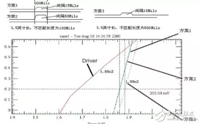
From the above simulation results, the waveforms of scheme 1 and scheme 2 are almost coincident, that is, the effect of unequal spacing is negligible. In comparison, the length mismatch does not affect the timing much. (Option 3). From a theoretical point of view, even though the inconsistent spacing will cause the differential impedance to change, because the coupling between the differential pairs is not significant, the impedance variation range is also very small, usually within 10%, which is equivalent to only one The reflection caused by the hole does not have a significant effect on signal transmission. However, once the line length does not match, a shift occurs in timing, and a common mode component is introduced into the differential signal to reduce the signal quality and increase the EMI.
It can be said that the most important rule in the design of PCB differential traces is the matching line length. Other rules can be flexibly handled according to design requirements and practical applications.
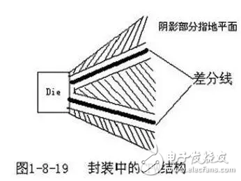
Myth #3: Think that the differential route must be very close. Making differential traces closer to nothing more than to enhance their coupling can both improve the immunity to noise and also make full use of the opposite polarity of the magnetic field to cancel the electromagnetic interference to the outside world. Although this approach is very favorable in most cases, it is not absolute. If we can ensure that they are adequately shielded from outside interference, then we do not need to make the anti-interference through strong coupling with each other. And the purpose of suppressing EMI. How can we ensure that differential traces have good isolation and shielding? Increasing the spacing from other signal traces is one of the most basic approaches. The electromagnetic field energy decreases with the square of the distance. When the line spacing is more than 4 times the line width, the interference between them is extremely weak. Can be ignored. In addition, the ground plane isolation can also play a good shielding effect, this structure is often used in high-frequency (10G and above) IC package PCB design, known as the CPW structure, can ensure strict differential impedance Control (2Z0), as shown in Figure 1-8-19.
Differential traces can also go in different signal layers, but this method is generally not recommended because different layers such as impedance and via difference will destroy the effect of differential mode transmission and introduce common mode noise. In addition, if the coupling between adjacent layers is not tight enough, the ability of the differential traces to resist noise will be reduced, but crosstalk is not a problem if the proper spacing from the surrounding traces can be maintained. In general frequencies (below GHz), EMI will not be a serious problem. Experiments have shown that 500Mils differential traces have a 60 dB attenuation of radiant energy beyond 3 meters, which is enough to meet the FCC electromagnetic emission standards. Designers do not have to worry too much about differential coupling due to insufficient electromagnetic compatibility.
3. Snake lineSerpentine lines are a type of routing often used in layouts. Its main purpose is to adjust the delay to meet the system timing design requirements. Designers must first have this understanding: serpentine lines will destroy the signal quality, change the transmission delay, and try to avoid using it when wiring. However, in actual design, in order to ensure that the signal has sufficient hold time, or to reduce the time offset between the same group of signals, it is often necessary to intentionally perform winding.
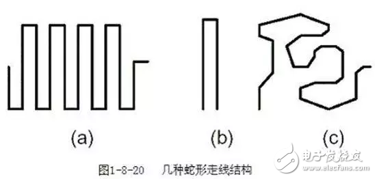
So, what effect does the serpentine line have on signal transmission? What should you pay attention to when you route? The two most important parameters are the parallel coupling length (Lp) and coupling distance (S), as shown in Figure 1-8-21. Obviously, when the signal is transmitted on the serpentine traces, coupling between the parallel lines will occur in differential mode. The smaller S is, the larger Lp is, the greater the degree of coupling will be. It may lead to a reduction of transmission delay and greatly reduce the signal quality due to crosstalk. For the mechanism, reference can be made to the analysis of common-mode and differential-mode crosstalk in Chapter 3.
Here are a few suggestions for Layout Engineers handling serpentine lines:
1. Try to increase the distance (S) between parallel lines, at least greater than 3H, and H refers to the distance the signal is routed to the reference plane. The popular saying is to walk around the big bend. As long as S is big enough, it can almost completely avoid the mutual coupling effect.
2. Decreasing the coupling length Lp, when twice the Lp delay approaches or exceeds the signal rise time, the resulting crosstalk will reach saturation.
3. The signal delay caused by the strip-line or the serpentine line of the Embedded Micro-strip is smaller than the micro-strip. In theory, the stripline will not affect the transmission rate due to differential mode crosstalk.
4. For high-speed and signal lines with strict timing requirements, try not to use a serpentine line, especially in a small area.
5. You can often use serpentine traces at any angle, as shown in Figure 1-8-20 C structure, can effectively reduce the mutual coupling.
6. In high-speed PCB design, the serpentine line has no filtering or anti-jamming capability and can only reduce the signal quality. Therefore, it is only used for timing matching and has no other purpose.
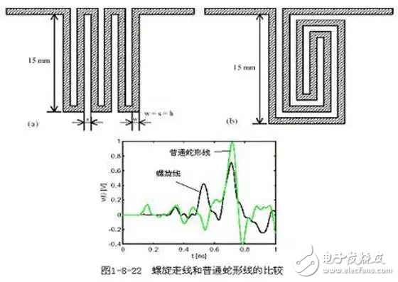
7. Sometimes the winding can be considered in the way of spiral routing. Simulation shows that the effect is better than the normal snake trace.
Camera Cable,Dash Cam Power Cable,Car Camera Cable,Power Cord of Tachograph
Dong guan Sum Wai Electronic Co,. Ltd. , https://www.sw-cables.com