PART– 0 basics
Before talking about MOS, let's recall semiconductor materials. As shown below:
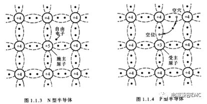
Take notes:
N-type semiconductor impurities are P atoms, many sons are electrons
P-type semiconductor impurity is B atom, many sons are holes
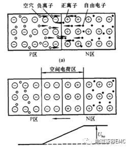
Since there are many free-moving atoms in the impurity semiconductor, when the N-type semiconductor is in contact with the P-type semiconductor, multiple sons undergo diffusion motion, and the free electrons and the free holes recombine to form a space charge region, which is also known as a depletion layer. .
Make another note: There are no freely moving conductive particles in the depletion layer.
The charging process of the junction capacitance of the PN junction can actually be regarded as complementing the free charged particle of the depletion layer.
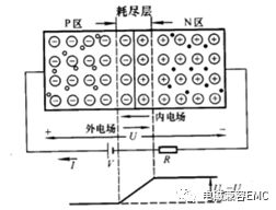
Applied voltage:
When the positive bias voltage of the PN junction is higher than the voltages of the barrier regions at both ends of the PN junction, the depletion layer conductive particles are completed and can have the same conductivity as the normal impurity semiconductor, and the circuit is turned on.
On the contrary, if the PN junction is connected with a reverse bias voltage, the depletion layer expands and the circuit is turned off.
PART-1 MOS tube structure

The MOS tube is introduced below, and the enhanced N-MOSFET is used as an example.
Enhanced N-MOSFET, full name: N-channel enhancement type insulated gate field effect transistor, before explaining its structure, the reader is reminded of several key words:
1 N-channel
2 Insulated gate
3 Enhanced
4 body diode
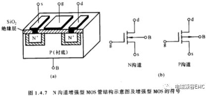
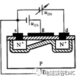
As shown in the structural diagrams we are familiar with in the Model Book (Tong Shi Bai, Fourth Edition), the structure of an N-channel enhancement MOSFET can be viewed as:
On a P-type semiconductor substrate, two N-type semiconductor regions are formed and two metal electrodes are used as the source S and the drain D; an insulating layer of SiO2 is formed on the P substrate, and a metal electrode is additionally provided as Gate G.
Its structural characteristics can be interpreted as the following points:
Since a N-type semiconductor is directly applied to a P-type semiconductor substrate, a depletion layer is formed between the two N regions and the P region.
2 Since the gate G is added on the SiO2 insulating layer, it is not conductive with the P-type semiconductor substrate, only the electric field effect
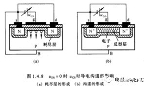
3 After the electric field is applied to the grid G, free electrons in the P-type semiconductor are attracted, and the depletion layer is filled at the same time, an inversion layer conductive channel is formed, and two N-type semiconductor regions are connected to make the enhancement N-MOSFET conductive.
4 When fabricating an N-MOSFET in a process, a source S is directly connected to a P-type semiconductor substrate, a source S is equivalent to a P-type semiconductor substrate, and there is a PN junction between the N-type semiconductor region of the drain D. The PN junction is the body diode of the N-MOSFET.

5 As shown in the above figure, there is a parasitic capacitance between the electrodes of the enhanced N-MOSFET, where the capacitance Cds between the source S and the drain D is its output capacitance, and the junction capacitance of the body diode position PN junction is structurally configured. The sum of the parasitic capacitances Cgd and Cgs between the grid G ​​and the S and D poles is the input capacitance, which is essentially the electrons that form the inversion layer and attract the electrons (as to why it is divided into two capacitors. The switching process of the MOS transistor is explained below) Continue to explain).
PART-2 MOS Controller Pass Through
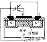
The conduction process of the MOS tube is actually the process of forming the inversion-type conductive channel.

Looking back at this picture, when a positive bias voltage Vgs is applied between the gate G and the source S, the electrons in the P-type semiconductor substrate of the enhanced N-MOSFET are affected by the electric field and are attracted to the gate. Simultaneously connect two N-type semiconductor regions to form an inversion layer conductive channel.
! Hit the blackboard! Plan focus!
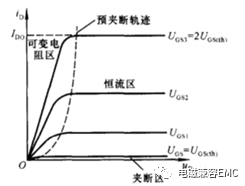
The positive bias voltage Vgs when the conductive channel is just formed is referred to as the turn-on voltage Vgs(th) (or “threshold voltageâ€); the voltage range where Vgs is greater than Vgs(th) is called the variable resistance region. The on-resistance of the drain D to the source S of the MOS transistor decreases as Vgs increases. After Vgs is greater than 2×Vgs(th), the on-resistance Rds-on is basically considered to be the lowest, s and when the temperature is uniform Staying the same, the enhanced N-MOSFET is now considered fully turned on. As shown below

Therefore, when setting the switching MOS transistor driving voltage, it is generally set to be much larger than 2×Vgs(th).
A set of graphs is given in the book to illustrate the effect of increasing the Vds on the current iD flowing through the MOS tube when Vgs is greater than the turn-on voltage.
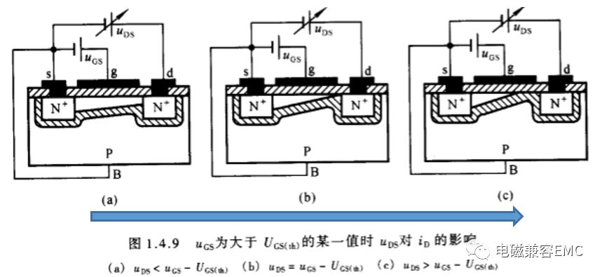
In fact, the order of the maps is reversed, which can simulate the course of the inversion layer of the MOS tube opening process approximately.
MOS tube conduction process can be roughly understood as:
1 Due to the effect of the electric field, an inversion layer near the source S region is formed first, so that the drain D to the source S of the MOS transistor can conduct and flow the current iD.
When the 2iD begins to flow, the inversion layer gradually expands toward the drain D, and finally makes the width of the inversion layer close to the drain D substantially equal to the width of the inversion layer near the source S.
3 The inversion layer continues to expand and Rds-on has been reduced to full conduction and remains unchanged.
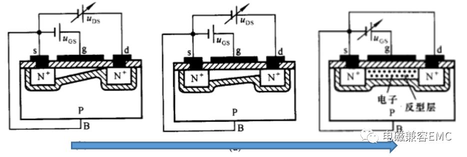
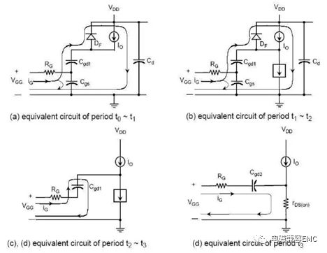
During the process of charging Cgd, Vgs remains unchanged. At this time, the Rds-on is large. When the current iD is certain, the MOS tube losses are large.
When the gate G receives an external voltage and the MOS transistor conducts the pass, the interval in which the Vgs remains constant is called the Miller interval. The phenomenon of Vgs, Rds-on, and MOS tube loss change due to the formation of the inversion layer is called Miller effect. The following describes the Miller effect in detail with the waveform.

This is a picture cut off from a blog in the forum. It has vividly reflected the changes in the current and voltage of the MOS tube when the gate drive number is applied.
(See the original text link)
T0-t1: The MOS transistor is not conducting because the gate voltage has not reached the turn-on voltage, as shown below
T1-t2: Vgs reaches the turn-on voltage, the MOS transistor starts to conduct, the inversion layer continues to widen, and the gate voltage continues to increase, as shown in the following figure:

T2-t3: The MOS transistor is located in the variable resistance region, and it is continuously turned on. The inversion layer is broadened toward the drain side (almost as shown in the red area in the figure below). The gate voltage is unchanged and enters the Miller platform:

T3-t4: When the inversion layer is basically widened to the same width, the gate continues to apply the driving voltage, and the entire inversion layer is widened until the gate voltage Vgs is consistent with the driving signal source, and the on resistance Rds-on:
If we look at the MOS model, we can see that the input capacitance Ciss of the inversion layer is divided into two capacitances, Cgs and Cgd, because the charge sequence of the two is different:
PART-3MOS tube parameters
I believe that readers are familiar with the parameters of the MOS tube, and will not be described in detail here. Referring to the description given in the blog above, only some of the parameters are supplemented here:
1), Absolute Maximum Ratings of Power MOSFETs:
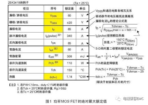
Note 1: The maximum drain-source voltage, VDSS, can be considered as the voltage applied across the body diode in the opposite direction, so there is only one direction.
Note 2: The gate-source maximum voltage VGSS, that is, the voltage applied between the gate electrode and the source electrode, due to the SiO2 insulating layer added to the gate and P-type semiconductor substrate, as long as the absolute value of the voltage exceeds the withstand voltage of the insulating layer It will break down, so there are two directions "±".
Note 3: The maximum drain current ID is the same as the value of the reverse drain maximum current IDR (or IS) flowing through the body diode. This is the same value as in the general specification. It is the PN flowing through the N-type semiconductor and the P-type semiconductor substrate. The maximum current of the junction.
Note 4: ID (pulse) needs to see the pulse width of the applied current, and the pulse width cannot follow the specification data.
Note 5: Avalanche current IAP also requires attention to the pulse width.
2) Static electrical characteristics
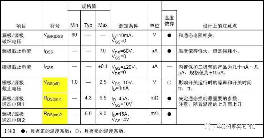
Note 1: Vgs(off) is actually the turn-on voltage Vgs(th), but the angle is different here.
Note 2: Readers who read the previous article should know why there are differences in the two Rds(on) sizes. Do not know to go back and look ahead.
3), dynamic point characteristics

Note 1: Ciss = Cgs + Cgd ; Coss = Cds ; Crss = Cgd
Note 2: The most important parameter for MOS tube startup speed is Qg, which is the total amount of charge needed to form an inversion layer!
Note 3: The on/off delay time td (on/off) and the rise/fall time tr / tf are determined based on the actual drain circuit ID and the gate drive voltage Vg when used in each project.
The introduction of MOS is basically as above, and the time and space relationship does not involve specific circuit explanation. The map source and the main reference books are "Analog Electronic Technology Foundation, (Tong Shi Bai. 4th Edition)", "Electronic Technology Fundamentals. Simulation Part. (Kang Wah Kwong. 5th Edition)". When engineers are working, they will read more about college textbooks. Sometimes there are different gains.
Diesel generator assembly by diesel engine, alternator, radiator, controller, base frame;
. World famous diesel engine brand: Cummins, Perkins, MTU, Kubota, Yuchai, Mitsubishi, Deutz, Doosan, MWM, GE, CRRC, Etc
. World famous AC alternator brand: Stamford, Leroy Somer, Mecc Alte, Marathon, Faraday, SWT
. World famous genset controller brand: Deepsea, ComAp, Deif, SmartGen,
. Good Quality Cooling Radiator
. Start Battery System
. Fuel Supplying System
. Filtering System
. Intake and Exhaust System
Diesel Genset,Diesel Generator,Diesel Generator Set,Portable Diesel Generator
Guangdong Superwatt Power Equipment Co., Ltd , https://www.swtgenset.com