According to the development layout of "One Core Park, Multiple Radiation Zones", Jiangmen High-tech Industrial Development Zone is the core park, and the Hetang Lighting Industrial Park, Heshan Gonghe Industrial Park and Taishan Industrial Park in Pengjiang District are radiated. The way of co-construction between provinces and cities, strive to build the city into an influential green (semiconductor) light source industry base at home and abroad, so that the green (semiconductor) light source industry will become the pillar industry of the city's industry, and strive to become a national-level green (semiconductor) ) Light source industry base.
Partial support policy
· New or expanded investment projects for the purchase of more than 5 (including 5) new MOCVD equipment (Specifications: blue-green MOCVD 31-chip machine and above, red-yellow MOCVD 38-piece machine and above) for the production of LED epitaxial wafers Fund subsidies. The blue-green light MOCVD subsidy fund is 10 million yuan/set, and the red and yellow light MOCVD subsidy fund is 8 million yuan/set.
· Corporate investors, innovative leaders (teams), senior managers and senior technicians (with doctoral degree, degree or senior title) who have made significant contributions to the development of the LED industry, 100% of the personal income tax local retention is used for awards Individuals; each year, another LED special contribution award of 2 million yuan will be set up to reward individuals or teams with special contributions (the specific measures will be formulated separately).
· A new investment project involving LED substrate production, epitaxial wafer production, and LED chip production. If the factory is completed within one year after signing the investment contract and is officially put into operation within 18 months, the construction area of ​​the completed plant will be subsidized by 100 yuan/square meter. . It belongs to LED chip packaging investment project, and the subsidy of 50 yuan/square meter meets the above conditions.
Information reference
Jiangfu [2009] No. 41 Document - Development of Green (Semiconductor) Light Source Industry Development Plan (2009-2015)
Jiangfu [2009] No. 36 Document - Temporary Preferential Measures for the Development of LED Industry in Jiangmen City to Promote High-tech Industrial Development Zone

SMT Stencils
The sole purpose of an SMT stencil is to transfer solder paste to a bare Circuit Board. A stainless steel foil is laser cut creating an opening for every surface mount device on the board. Once the stencil is properly aligned on top of the board, solder paste is applied over the openings (making a single pass, using a metal squeegee blade). When the stainless steel foil is separated from the board, solder paste will remain, ready for placement of the SMD. This process, as opposed to hand soldering methods, ensures consistency and saves time.
Stainless steel foil thickness and aperture opening size control the volume of paste deposited on the board. Too much solder paste causes solder balling, bridging, and tomb-stoning. A lack of solder paste creates insufficient solder joints. All of which compromise the electrical functionality of the board.
Proper foil thickness is
chosen based on the types of devices being loaded on the board. Component
packages such as 0603 capacitors or 0.020" pitch SOICs, will require a thinner
solder paste stencil than larger packages such as 1206 capacitors or 0.050"
pitch SOICs. Solder paste stencil thickness ranges from 0.001" to 0.030". The
typical foil thickness used on the majority of boards is anywhere from 0.004"
to 0.007".
Now offering nano coating on select stencils and sizes! "Nano
coating" is a two part, wipe on process, made up of hydrophobic elements that
repel flux and solder, resulting in improved paste release for extremely small
components. The coating is applied to the contact side of the stencil prior to
shipment, making the stencil ready to use right out of the box. This coating is
recommended for fine pitch QFN`s, fine pitch IC`s, micro BGA`s, and 0201
component types.
Framed SMT Stencils
Framed Stencils or glue-in stencils are laser cut stencil foils permanently mounted in a stencil frame using a mesh border to tightly stretch the stencil foil taut in the frame. These solder paste stencils are designed for high volume screen printing on printed circuit boards. They are recommended for Printed Circuit Board assembly when doing production runs. Our framed stencils provide optimum solder pastevolume control. Framed stencils have smooth aperture walls and can be used for 16 Mil pitch and below and for Micro BGAs.
Frameless SMT Stencils
Frameless Stencils are laser cut stencilsdesigned to work with stencil tensioning systems also known as Reusable Stencil Frames like the Universal Frame These solder paste stencils do not need to be permanently glued in a frame. Frameless Stencils are significant less expensive than Framed Stencils and reduce storage space requirements.
Frameless Stencils are designed for screen printing on Printed Circuit Boards. They are recommended for prototype printed circuit board assembly or short runs. Our Frameless Stencils provide optimum solder paste volume control. They have smooth aperture walls and can be used for 16 Mil pitch and below and for Micro BGA's.
Prototype SMT Stencils
Prototype Stencils (standard to 10"x12") are laser cut stencils custom-made for your own printed circuit boards using your Gerber Paste file. Comes with a squeegee blade and board holders. These frameless solder paste stencilswere specially designed for manual printing.
Rayming produce Solder Paste Stencils - Laser Cut Stencils,SMT stencils, and offers the largest selection of SMT stencils.
About Us:
BentePCB is a professional PCB manufacturing which is focus on double side, multilayer, HDI PCB , rigid PCB and Flexible PCB mass production. The company was established on 2011.
We have two factories together, The factory in Shenzhen is specialized in small and middle volume orders and the factory in Jiangxi is for big volumn.
Why Us?
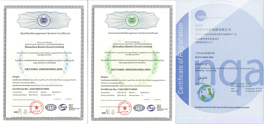
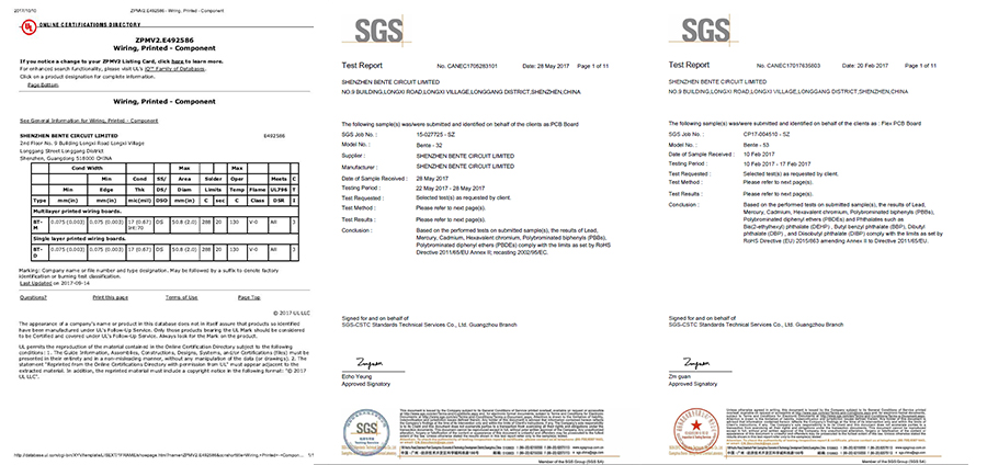
UL (E492586), ISO9001, ISO14001, TS16949, RoHS certified.
Turnover USD 10-50 million per year.
15,000 sqm area, 450 staff .
Mass Production from single to 16 layers.
Special Material:ROGERS, Arlon, Taconic.etc.
Client:Huawei, SAMSUNG, Malata, Midea,Texas Instruments.etc.
Certification(UL:E492586, TS16949, ISO14001, ISO9001,RoHS):
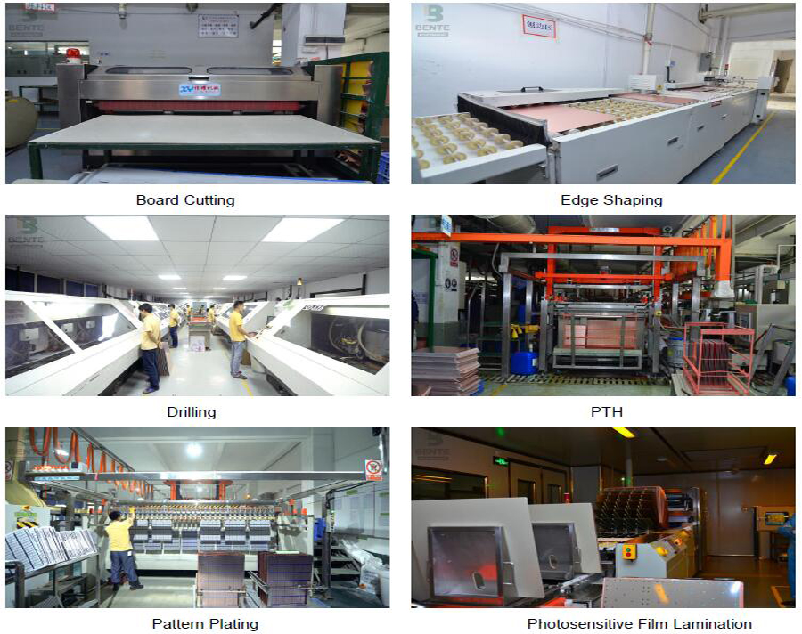
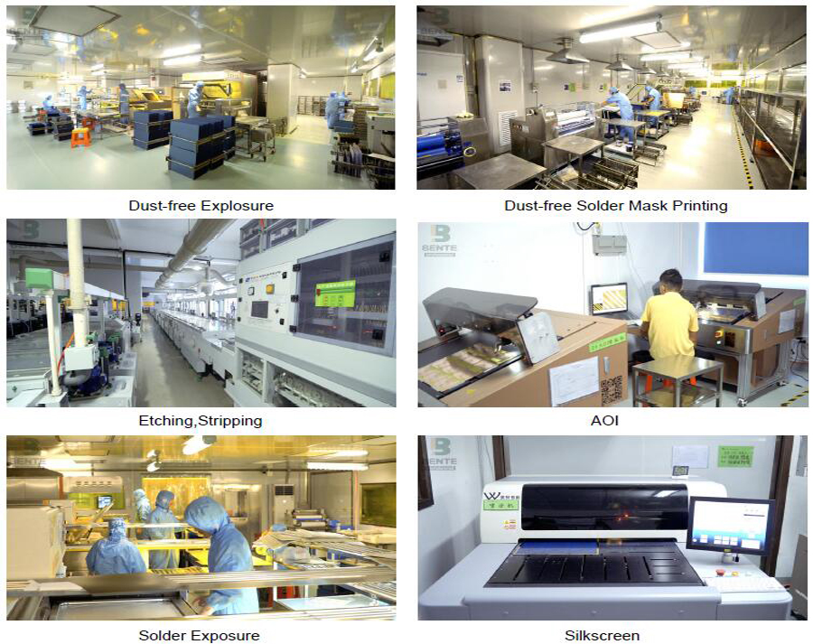
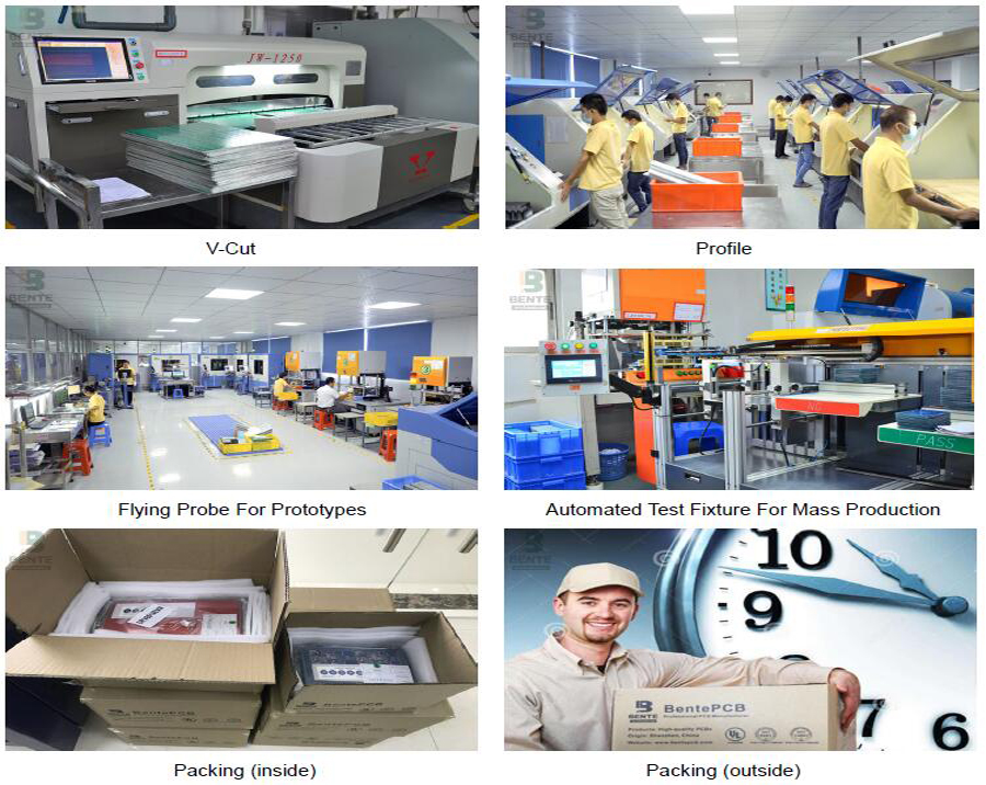
Factory Tour:
Exhibition:
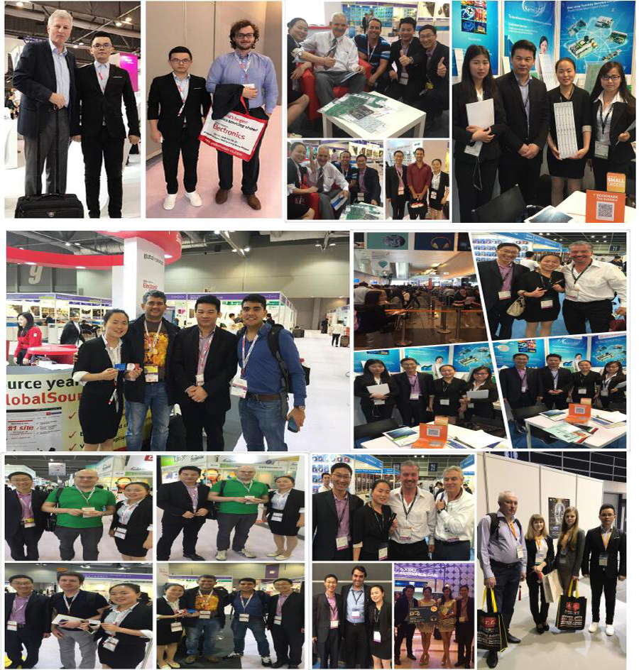
We Took part in the famous exhibitions over the past years,and got highly appreciation from the top experts,as well as cooperated tightly with them.
Delivery:
BentePCB offers flexible shipping methods for our customers, you may choose from one of the methods below.

FAQ:
Q1: What does BentePCB need for a customized PCB order?
A: The customers need to provide Gerber or pcb file.If you do not have the file in the correct format, you can send all the details related to the products.
Q2: What is your quotation policy?
A: For the PCB order in large quantity, BentePCB will send you the quotation based on the MOQ of the products concerned, and the price will be reasonable with good quality.
Q3: How long will you send us quotation ?
A: After all files were sent, 2 to 8 hours as per your file.
Q4:What is your minimum order quantity?
A:Our MOQ is 1 PCS.
Q5: How about the service BentePCB offered to the customers?
A: If you have any questions about our products or company, do not hesitate to send us your inquiry toour customer service representatives, Your satisfaction is our pursuits.

We don`t just sell PCBs .We sell sleep.

SMD Stencil
SMD Stencil, PCB Stencil, SMT Stencil, Stencil Printer
Shenzhen Bente Circuit Limited , http://www.bentegroup.com