The history of programmable logic devices The development of programmable logic devices can be divided into four phases, from the early 1970s to the mid-1970s, the first phase, and the mid-1970s to the 1980s, the second phase. It was the third stage from the 1980s to the end of the 1990s, and the fourth stage from the end of the 1990s to the present.
The first stage of the programmable device is only three kinds of simple programmable read-only memory (PROM), ultraviolet erasable read-only memory (EPROM) and electrically erasable read-only memory (EEPROM). Due to structural limitations, they can only Complete simple digital logic functions.
In the second phase, there are structurally slightly complex programmable array logic (PAL) and general array logic (GAL) devices, which are officially called PLDs and can perform various logic operations. A typical PLD consists of an AND and a non-array array, and an AND or OR expression is used to implement any combinational logic, so the PLD can perform a large number of logical combinations in product and form.
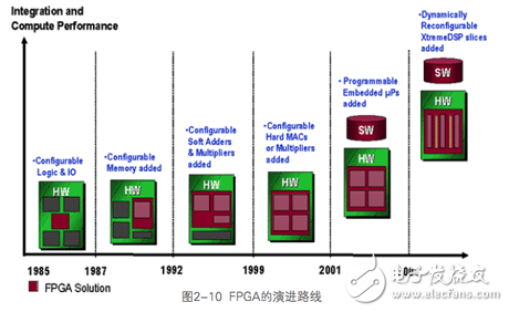
Phase 3 Xilinx and Altera have introduced an FPGA similar to a standard gate array and an extended CPLD similar to a PAL structure, which improves the speed of logic operations, has flexible architecture, logic unit, high integration and wide application range. It is compatible with the advantages of PLD and general-purpose gate arrays. It can realize ultra-large-scale circuits and flexible programming methods. It is the first choice for product prototype design and small and medium-sized (generally less than 10,000) products. At this stage, CPLD and FPGA devices have made great progress in manufacturing process and product performance, reaching a scale of 0.18 process and multi-million gates.
The fourth phase of SOPC and SOC technology, the result of the integration of PLD and ASIC technology, covers the real-time digital signal processing technology, high-speed data transceiver, complex computing and embedded system design technology. Xilinx and Altera also introduced the corresponding SOCFPGA products with a manufacturing process of 65nm and a system gate count of more than one million gates. Moreover, this stage of the logic device embedded with hard core high-speed multiplier, Gbits differential serial interface, PowerPC? microprocessor with clock frequency up to 500MHz, soft core MicroBlaze, Picoblaze, Nios and Nios II, not only realize the software requirements and The perfect combination of hardware design also achieves the perfect combination of high speed and flexibility, which has surpassed the performance and scale of ASIC devices, and surpassed the concept of FPGA in the traditional sense, making the application range of PLD extended from monolithic to system. level. In the future, Xilinx executives revealed that the company is developing a new FPGA with a new process, which will integrate larger memory cells and other functional devices, and FPGAs are moving toward super system chips! On February 5th, Xilinx released the Spartan-6 and Virtex-6 FPGA series using 40nm and 45nm, and opened the new design concept of the target design platform. It is believed that the application of FPGA will be further developed!
1080P Home Projector-1080P high-definition picture presentation, immersive experience, leisure and entertainment, enjoy games, videos, TV series, photos, sports, UEFA Champions League, etc. Mini portable projector, small and light, to carry and use, environmentally friendly micro LED flat light source design extremely long life
1080P Home Projector,Home Cinema Projectors,Projector For Room,Tv Projectors
Shenzhen Happybate Trading Co.,LTD , https://www.happybateprojector.com