TLE8201
TLE8201 is a highly integrated power ASSP (special standard product) for door modules. This includes the power levels necessary to drive loads in typical front door applications, such as center door locks, deadlock or mirror folding, mirror positioning, mirror heating, and 5W or 10W lights or LED (Such as turn signal lights, door-controlled cabin lights / safety warning lights or control panel lights), etc. 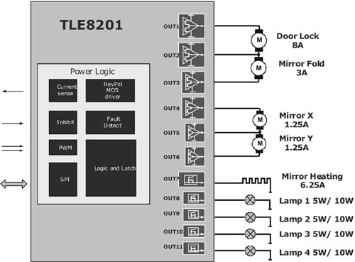
Figure 1 TLE8201 block diagram
The TLE8201 has short-circuit and over-temperature protection functions and complete diagnostic functions that comply with automotive application safety regulations. The current sensing output can improve the overall performance of the system.
The standard SPI interface not only reduces the length of the microcontroller's I / O lines, but also allows flexible control of the power stage and provides complete diagnostic functions.
TLE8201 has two PWM inputs, both of which are direct power stage control inputs, which can enhance the flexibility of PWM mapping. The information in the SPI register defines the power level to be controlled by the PWM input. The PWM function can be configured to support up to eight power transistors.
The device is packaged in Power-SO and equipped with a large heat sink, so it has good thermal resistance performance. The pins are optimized to achieve efficient PCB design. The application of TLE8201 not only helps to save PCB area and cost, but also enhances the system quality and improves the output.
TLE8201 application circuit
Figure 2 shows the application circuit of TLE8201 in the door control module.
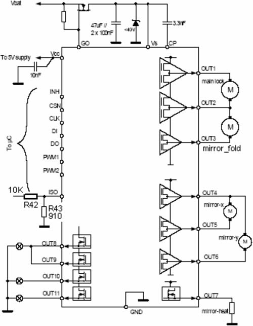
Figure 2 Application circuit
power supply
TLE8201 has two power input terminals: all power drivers are connected to the power supply voltage Vs pin connected to the 12V power line of the car. The internal logic circuit part is powered by an independent 5V Vcc voltage. In this way, even if a short-term power outage occurs in Vs, it can ensure that the information stored in the logic circuit is not affected.
TLE8201 requires external reverse polarity protection. It is equipped with a charge pump output for connecting external n-channel logic level MOSFETs. The connection method of the protection circuit is shown in Figure 2, the gate voltage is provided by the pin GO.
By setting the INH input to "low", the TLE8201 can be placed in a low-power mode. In sleep mode, all output transistors are turned off and the SPI stops working. In this mode, the maximum value of total quiescent current is only 6μA (Vs and Vcc).
SPI
SPI is used to realize two-way communication with the control unit. When the chip is selected by the CSN (chip-select-not) input (H to L) mode, the transmission cycle is started. The 16-bit control word is read through the DI serial data input. The status word is displayed synchronously on the DO serial data output. Synchronous communication is realized through the serial clock input terminal CLK.
As shown in Figure 3, the 16-bit SPI framework consists of an addressable block, an address independent block, and a 2-bit address, including two control registers and two diagnostic registers. The independent address input section is used for general settings, and the independent address output section is used to mark errors and record temperature information. 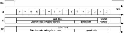
Figure 3 SPI structure
PWM input
PWM-ing is a very flexible function provided by TLE8201. Two PWM modes can be configured to control the required power level: connect the PWM1 and PWM2 pins to the timer channel of the microcontroller, and then select the desired HSsel bit to activate the PWM function. It is recommended to set the PWM frequency below 200 Hz to minimize the power consumption caused by switching losses.
Current sensing
The ISO (inductive output) pin provides a current proportional to the output current flowing to GND at the selected power output. The output selection is realized through SPI.
The induced current is converted into a voltage by an external sensing resistor R43 and sent to the input of the A / D converter.
Output stage
Outputs 1-6 are half-bridges, and outputs 7-11 are high-side switches. The latch motor and rearview mirror folding motor can be connected to output 1, output 2 and output 3. Output 2 is the sum of the two motor currents. Two rearview mirror positioning motors are connected to output 4, output 5 and output 6. High-side driver output 7 is used to drive the mirror heater. Output 8 and output 9 are used to drive 5W lights. The output 10 can be connected to the output 11 to jointly drive 10W headlights.
Latch control
start up
Both output 1 and output 2 of the TLE 8201 are connected to the latch motor. The microcontroller in the door control module communicates with the TLE 8201 via SPI. After the power is turned on, the door lock status is either received by the body control module and transmitted to the door control module, or directly received by the door control module through LIN or CAN. When the door or switch panel sends a switch input request or receives a CAN / LIN message from BCM, the latch motor is activated.
Figure 4 shows the starting waveform of the latch motor. Channel 1 is the current flowing through the latch motor. Channels 2 and 3 are the voltage output of output 1 and output 2 in TLE 8201. When PWM soft start is not used, the startup surge current may reach 2A. After starting, the current will drop to about 0.8A. When the latch is fully closed or opened, if the motor stalls, the latch motor can be automatically shut down. When detecting the motor stall, the motor current can be measured through the ISO output of the TLE 8201; this output is connected to the grounding sense resistor R43, and to the MCU analog input through the protection resistor R42.
The calculation method of the block detection standard is as follows:
KILIS12 = 2000, R43 = 910ohm, according to the waveform, the minimum block current is IOUT = 2.5A; then, the block detection voltage can be calculated: block detection voltage (Vblock-detecTIon) = IISO * R43 = IOUT / KILIS12 * R43 = 2.5A / 2000 * 910V / A = 1.1375V
After detecting the block voltage, switch HS1 and HS2 to the "high" position to make the motor enter the freewheeling mode. Both HS1 and HS2 remain high for 100 milliseconds. When switching from L to H, a minimum dead time of 3 microseconds will occur to ensure that switching slope overlap does not occur, thereby avoiding cross current.
During the freewheeling process, there will be a small current, which is the result of the special mechanical structure of the latch motor. There is a spring in the latch to protect the latch from damage, otherwise, the latch will slam the upper part of the door lock.
The following is the voltage calculation formula of ordinary DC motor: 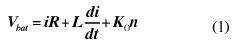
Among them, Vbat means external voltage; i means motor current; L means motor inductor; n means motor speed; R means internal motor resistance.
When the motor is running at almost constant speed, Vbat = iR + K0n (as shown in Figure 1). It should be pointed out that K0n represents the back electromotive force of the motor.
When the motor starts freewheeling, 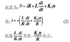
After the freewheeling, because there is no motor current (ie, there is no motor torque), the spring will push the latch motor back slightly. In other words, the speed of the latch motor will change from zero to a negative value, thereby generating a positive current through the motor. 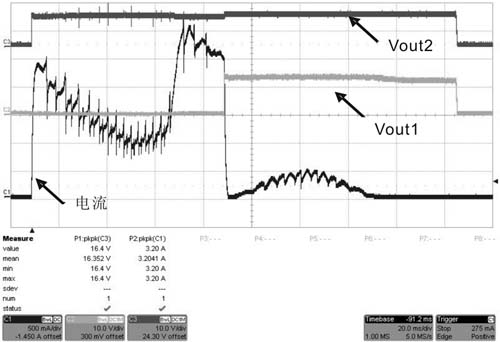
Figure 4 Latch start waveform
Protection and diagnosis
In the ON-state, the load detection can be enabled through the low-side switch of the bridge output: when the current through the low-side transistor is lower than the reference current, and the time that the IOCD is in the startup state exceeds the open load detection delay tdOC The corresponding open load diagnosis bit will be set. However, the output transistor remains activated. The error bit for turning on the load is locked and can be reset through the SPI status register reset or power-on reset.
Rearview mirror folding control
normal operation
Rearview mirror folding motor is driven by output 2 and output 3 of TLE8201. Because the half-bridges are connected in series, and the channel current is also limited, only one motor can be driven at a time. So as long as the latch motor is running, the rearview mirror folding output cannot be started.
Figure 5 shows the waveform of the rearview mirror folding motor during normal operation. Channel 1 is the current flowing through the rearview mirror folding motor. Channel 2 is the voltage of output 3, and channel 3 is the voltage of output 2. According to this waveform, the maximum value of the surge current at startup is 2.52A, while the rated current during operation is 0.4A. 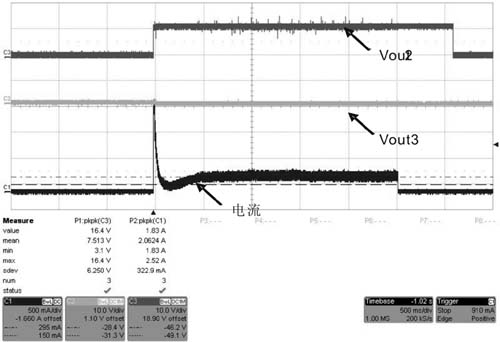
Figure 5 Waveform of rearview mirror folding motor during normal operation
The motor will keep running until it locks or exceeds 3 seconds. Because the rearview mirror folding motor adopts a special mechanical structure, the load will appear when the motor is locked! Since the current during the locking process will drop to 0A, the motor does not need to continue.
Short circuit protection
Figure 6 shows the short-circuit protection behavior of TLE8201. The meaning of each channel is the same as in Figure 5. During normal operation, the voltage at output 2 (channel 3) is higher and the voltage at output 3 (channel 2) is lower. The rated current is 0.4A, which seems to be 0A in Figure 6.
When the motor terminal is short-circuited and the current exceeds output 3 (ISD34 is usually 4A) shutdown threshold ISD for more than shutdown delay tdSD, the output transistor of output 3 will be turned off and the corresponding diagnostic bit will be set. Since the short-circuit shutdown threshold of output 2 is higher than 8A, the output transistor of output 2 will continue to operate. Therefore, the voltage of output 3 will increase to a level equal to the voltage of output 2.
During the delay, the current value is limited to ISC output 3 (ISC34 is usually 6A). The delay is relatively short (usually 25 microseconds) in order to reduce the energy consumption when the device is short-circuited. This design can provide the peak current required in motor applications. Before sending the status register reset command to the SPI or performing a power-on reset, the output stage will remain off and set the error bit.
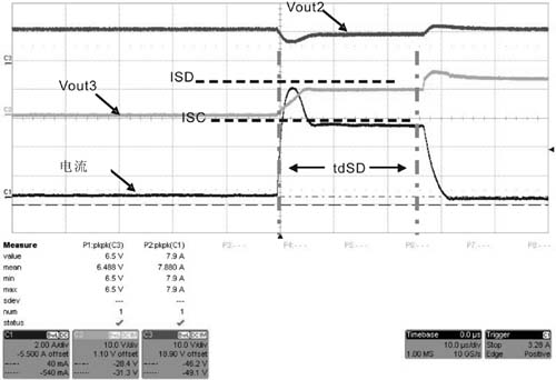
Figure 6 Short circuit protection behavior
Rearview mirror positioning control
Two motors are used, output 4 is connected to the X motor, output 5 is connected to the two motors, and output 6 is connected to the Y motor. Figure 7 shows the waveform of one of the rearview mirror positioning motors during normal operation.
Press the button to activate a state. When the rearview mirror folding motor is activated, the rearview mirror XY output cannot be activated. This type of output does not have PWM control. The surge current at startup is about 0.2A, while the rated current is 0.1A. Although there is no need to use active braking, the high-side switch will remain active for 100 milliseconds after the mirror moves.
Figure 7 shows the short-circuit protection behavior. The short-circuit protection theory used for outputs 1-6 is exactly the same. The only difference is that the short-circuit shutdown current threshold and the short-circuit current value are different. 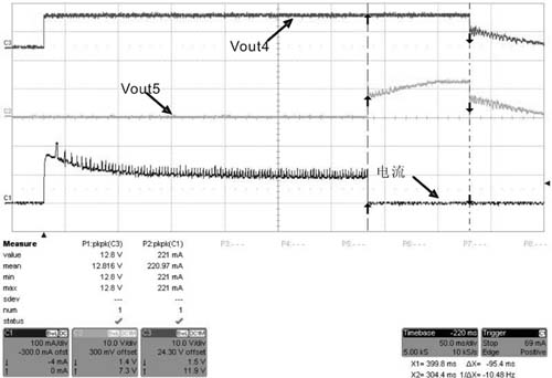
Fig. 7 Waveform of X-rearview mirror motor during normal operation
Figure 8 Short-circuit protection behavior
Rearview mirror defrost control
The PTC heating device is driven by TLE 8201 output 7. When the fixed 10 second turn-on time is exceeded, the output is controlled by low-frequency (eg 10 Hz) PWM, and the duty cycle is usually 40%. The control of PWM is realized by software through SPI. When the door lock is activated, the heater is turned off to reduce the overall current through the TLE 8201.
Car light control
normal operation
The door control lights and safety warning lights are driven synchronously by outputs 10 and 11 of TLE 8201. The output is turned on / off by 200 Hz PWM (theatre lighting effect) within 2 seconds. PWM is controlled by PWM2 input. The turn signal (10 w) is driven by outputs 8 and 9 of TLE 8201. The output is controlled by low frequency (eg 1.5 Hz) PWM, and the duty cycle is usually 50%. The control of PWM is realized by software through SPI.
Ground protection output short circuit
The ground protection output short-circuit behavior shows the difference between a short circuit that occurs during turn-on and a short circuit that occurs when it is turned on.
Short circuit during switch-on
In the process of turning on the output, the current and voltage levels are used to detect the presence of a short circuit. If the switch (such as output 8) is open and the short-circuit condition is valid, the current will exceed the shutdown threshold ISD8 (1.8A to 3.5A), and the output voltage will be lower than VSD8 (1.5V to 3.3V). When tdSDon8 (125 microseconds to 350 microseconds) is exceeded, the output transistor is turned off and the corresponding diagnostic bit is set. During the delay, the current value is limited to ISC8 (usually 4.2A), as shown in Figure 9. Channel 1 is the output current, and channel 2 is the output voltage.
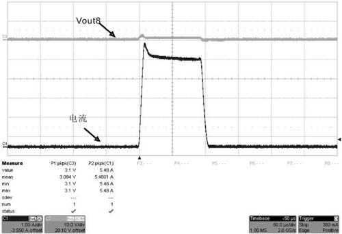
Figure 9 Waveform of short-circuit protection during the connection process
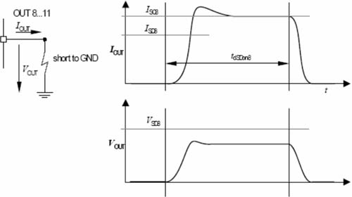
Figure 10 Short-circuit protection during switch-on
Short circuit in open state
If the switch has been opened and a short circuit has occurred, and the current exceeds the shutdown threshold ISD for more than the shutdown delay tdSD (10 microseconds to 60 microseconds), the output transistor will turn off and set the corresponding diagnostic bit. This mechanism has nothing to do with the voltage Vout. See figure 11.
Figure 11 Short-circuit protection in the open state
Turn on the load
Figure 12 shows the open load of the high-side switch in the closed state. Turn-on load detection is achieved by comparing the output voltage with the threshold VOpL. The pull-up current can be turned on or off by the OpLxON bit. If an output is used to drive the LEDs, the OpLxON bit should be set to "low", that is, the pull-up current is cut off, because these LEDs may emit light when the bias is applied by the pull-up current. 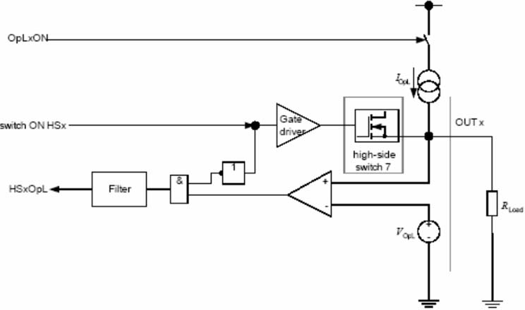
Zener Diode, the English name Zener diode, also known as Zener diode. By using the reverse breakdown state of the pn junction, the current can be varied over a wide range and the voltage is substantially constant, and the diode that acts as a voltage regulator is fabricated. [1] This diode is a semiconductor device that has a very high resistance until the critical reverse breakdown voltage. At this critical breakdown point, the reverse resistance is reduced to a small value in this low resistance region. The current is increased and the voltage is kept constant. The Zener diode is binned according to the breakdown voltage. Because of this characteristic, the Zener diode is mainly used as a voltage regulator or voltage reference component. Zener diodes can be connected in series for use at higher voltages, resulting in higher regulated voltages in series.
Zener Diode
Power Zener Diode,Zener Diode,Zener Diode Regulator,Zener Diode 56V
Dongguan Agertech Technology Co., Ltd. , https://www.agertechcomponents.com