Preface
Many older linear devices, especially op amps, referred to as "op amps", do not have a SPICE macro model. Even if there is, the Boyle macro model is usually used. The model is not accurate to today's standards, and even if it is provided to the user, it does not represent the actual device well.
This transistor-based approach uses relatively simple equations that engineers can modify to meet the needs of various amplifier design flows. Our philosophy is to create a SPICE (TINA-TITM) macro model with several parameters from the product specification, regardless of the input or output topology. The technique is based on the assumption that most op amps have a sub-pole that far exceeds the unity-gain bandwidth.
In general, engineers need the following parameters: supply voltage, open loop gain and load, unity gain bandwidth, slew rate, input common mode range, common mode rejection ratio (CMRR), power supply rejection ratio (PSRR), Vos, Ios, Ib, open-loop output impedance, phase margin, wideband noise and 1/f noise, supply current, and short-circuit current. For rail-to-rail outputs, engineers will need to output the saturation voltage (input and output voltage difference) as well as the sink and source currents. In addition, the load resistance RL needs to be specified.
Equations highlighted in different colors are equations that engineers need to insert into the netlist. The blue equation is for the convenience of the engineer to observe; the red equation is required for the model parameters at the end of the netlist.
Figure 1 shows the topology of a bipolar input and a complementary metal oxide semiconductor (CMOS) output stage.
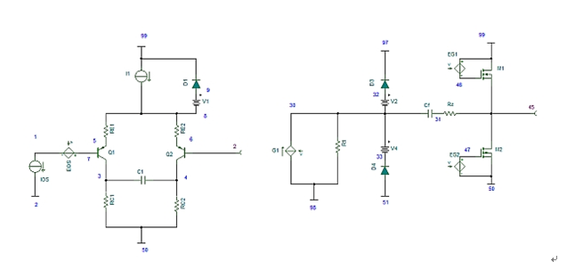
Figure 1: Three-level topology of a non-rail-to-rail bipolar input and a CMOS output op amp
Input stage
The input stage consists of: a differential pair (Q1/Q2); currents I1, D1 and V1 - they can set the common mode to a high level; Rc1 and Rc2; a C1 of the secondary pole can be set; RE1 as a negative feedback of the emitter And RE2; EOS - a voltage-controlled voltage source in series with a non-inverting input. This voltage source has several components. The first represents the input offset voltage; the second is associated with the common mode rejection ratio (CMRR); the third is associated with the power supply rejection ratio (PSRR), and so on.
Ios is a current source that represents the input offset current of the op amp.
The intermediate stage consists of a voltage-controlled current source G1 that corresponds to an arbitrary value of R1; D3/V3 – a higher voltage clamp can be set; D4/V4 for lower voltage clamps; EVp and Evn – — They can be used as power supplies for D3/V3 and D4/V4 respectively. EREF is a voltage-controlled voltage source that can be used to generate a reference node for a macro model. Finally, set a pole/zero with CF and Rz to help get the proper phase margin.
The output stage consists of two voltage-controlled voltage sources connected in parallel with two transistors.
The next step is to derive the necessary equations for the netlist to develop the macro model.
First determine I1 - the tail current from the input differential pair. This value can vary depending on the process technology employed. While an ideal engineer can request it from an integrated circuit (IC) designer, an engineer does not always have this option; therefore, it is best to set it to any number between 100μA and 1mA.
Set the LV voltage to 130 and the IS to 1E-16. Beta is expressed as BF1, which is equal to I1/2*Ib, where Ib is the input bias current value from the product specification.
If using a 5V power supply, then set the common mode to high with V1 = Vs-Vcm. The voltage rail provides a common-mode upper voltage of 1V, so set V1 to 1V.
Collector resistors RC1 and RC2 are set equal to 0.2 (VRC) multiplied by 2 and divided by I1.
For the emitter negative feedback resistors RE1 and RE2:
RE1 = RE2 = (BF1 * RC1-rπ * Avinput) (1)
among them
RÏ€ = [(BF1*VT*2)/I1], and Avinput = Aol*1000/(Avout*Avmiddle) (2)
Please note: VT = kT/q, where k is the Boltzmann constant (1.38E-23); T is the ambient temperature in Kelvin (K); q is the charge of an electron (1.6E-19) . At 300oK, VT = 25.9 or 26mv.
The final step in the input stage is to explore capacitor C1 across the input differential pair:
C1 = (1/2 * RC1 * p1), where p1 = 90 - ? m - fz (3)
In this equation, ?m is the phase margin from the product specification; fz is the hysteresis amount from Rz (the zero point in the intermediate stage), and fz = atan(GBP/fz) (expressed in degrees).
Please note: GBP is the unity gain bandwidth of the op amp, and fz is the zero point calculated in the intermediate level.
Let's summarize the information we have about the bipolar input stage so far:
Net table (macro model) required values:
I1 = 100e-6
VA = 130
IS = 1E-16
BF1 = I1/2*Ib
V1 = Vs-Vcm, high level
RC1 = RC2 = 2*VRC/I1
Optional: RE1 = RE2 = (BF1*RC1-rπ*Avinput)
C1 = (1/2 * RC1 * p1), where p1 = 90-?m-fz
The following is what the netlist looks like:
* Device pin configuration sequence +IN -IN V+ V- OUT
* Device Pin No. 1 3 5 2 4
* Node assignment
* Non-inverting input
* | Inverting input
* | | Positive power supply
* | | | Negative power supply
* | | | | Output
* | | | | |
* | | | | |
.SUBCKT MOCK 1 2 99 50 45
*
* Input level
*
Q1 3 7 5 PIX
Q2 4 2 6 PIX
RE1 5 8 4E3
RE2 6 8 4E3
RC1 3 50 68.5
RC2 4 50 68.5
I1 99 8 100E-6
C1 3 4 8.44E-13
D1 99 9 DX
V1 9 8 0.9
EOS 7 1 POLY(5)(73,98)(22,98)(81,98)(80,98)(83,98)0.5E-3 11111
IOS 1 2 1.1E-9
Please note that the first constant in the EOS term is the maximum input offset voltage of 500μV.
Intermediate level
In this section, R1 is arbitrarily set to 1 MΩ. The voltage controlled current source G1 can be calculated according to the following equation:
G1 = R1*Cf/(I1*RC1) (4)
Please note: Rc1 = Rc2.
Now you need to determine Cf, which is expressed as:
Cf = 1/2Ï€* fdom*R1*(Avout+1) (5)
Where fdom is the dominant pole and is expressed as GBP/Aol*sqrt(1+(Aol^2/p1^2)). GBP is the unity gain bandwidth of the op amp.
P1 = GBP/TAN(90-?m-2)
Fz = gm5+gm6/2Ï€*Cf
Gm5 = sqrt(2*kp*W/L5*Id)
Gm6 = sqrt(2*kp*W/L6*Id)
Id = 1/2kp*(W/L5)*(Vdc5-Vt5)*2*(1+?*Vs/2) (6)
Where kp is a process parameter called transconductance and should not be confused with gm.
Please note that gm5 and gm6 are different values ​​because W/L5 and W/L6 are independent of each other and are associated with the current gain β (β5 and β6) of each transistor.
Finally, set the clamp diode as follows:
V3 = 0.7 + Vs/2-V30max
V4 = 0.7 + Vs/2 + V30min
Where Vs is the supply voltage.
V30max = 2*Isink*Req-(VDC6-Vt6) (7)
Where Req is the input-output voltage difference when the current (the sink current) is 1 mA.
V30 min = 2*Isource*Req-(VDC5-Vt5) (8)
In this case, Req in equation (8) is equal to VDO - the current (source current) is 1 mA.
We will discuss the calculation of the VDC6-Vt6 and VDC5-Vt5 at the output stage.
The calculation formula of the intermediate gain AVmiddle is G1*R1*2.
The following is what the netlist looks like:
Gain level
G1 98 30(4,6)3.73E-03
R1 30 98 1.00E + 06
CF 30 31 8.1E-10
RZ 45 31 3.91E + 02
V3 32 30 2.14E + 00
V4 30 33 2.08E + 00
D3 32 97 DX
D4 51 33 DX
Rail-to-rail CMOS output stage
As shown in Figure 1, the output stage consists of a pair of P-type and N-type MOS transistors. Similarly, for a bipolar design, it will also have a pnp tube and an npn tube.
There are also two voltage-controlled voltage sources: EG1 and EG2 for PMOS and NMOS transistors.
Let's start with the output gain Avout:
Gm5*Req+gm6*RLeq
Req = rds5*RL/rds5+RL (9)
Where RL is the load resistance and rds5 = 1/?*Id.
Please note: Since the Id and Id are the same for both transistors, the NMOS Req and the PMOS Req are the same (Req = rds5*RL/rds5+RL).
W/L5=β5/kp
55=1/2*Isource*Req*2 (10)
Req is the input-output voltage difference when the current (for the PMOS, the source current; for the NMOS, the sink current) is 1 mA.
For NMOS, let's rewrite the equation as:
Rds5 = 1/?*Id
W/L6 = β6/kp
66 = 1/2*Isink*Req*2 (11)
In terms of device and process parameters, you will need the following information:
?= 0.01
VTO ​​= 0.328
KP = 1E-5
For rail-to-rail output stages, engineers will need maximum sink current and maximum source current (as specified by the product specification or designer):
Vdc5-Vt5 = 1/(Ro*β5+sqrt(β5*β6)) (12)
Where Ro is the open-loop output impedance.
Vdc6-Vt6 = Vdc5-Vt5*sqrt(β5/β6) (13)
The output level in the netlist should look like this:
* Output stage
M1 45 46 99 99 POX L = 1E-6 W = 3.20E-03
M2 45 47 50 50 NOX L = 1E-6 W = 2.78E-03
EG1 99 46 POLY(1)(98,30)3.684E-01 1
EG2 47 50 POLY(1)(30,98)3.714E-01 1
*
Process and device parameters are listed at the end of the model in the following manner:
* Model
*
.MODEL POX PMOS (LEVEL = 2, KP = 1.00E-05, VTO = -0.328, LAMBDA = 0.01, RD = 0)
.MODEL NOX NMOS (LEVEL = 2, KP = 1.00E-05, VTO = + 0.328, LAMBDA = 0.01, RD = 0)
.MODEL PIX PNP (BF = 625, IS = 1E-16, VAF = 130)
.MODEL DX D (IS = 1E-14, RS = 0.1)
.MODEL DNOISE D (IS = 1E-14, when RS = 0, KF = 1.21E-10)
*
.ENDS MOCK
Add CMRR and PSRR to your model
Adding CMRR and PSRR is as simple as a resistor-capacitor (RC) network with a voltage-controlled voltage source (Figure 2).
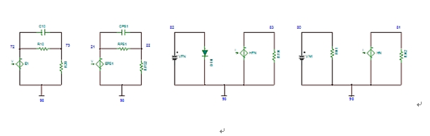
Figure 2. Simple Resistor Capacitor (RC) Network that Produces Small Signals CMRR, PSRR, and Noise (including Flicker Noise)
To simulate these, all the information we need is: DC value, pole and zero position, which can be found in the diagram of the product manual.
E1 = [10^ -(CMRR/20)*(Zero/Pole)]/2 (14)
In terms of CMRR:
Where CMRR is the DC value (in dB) and the unit used for zero and pole is Hz.
R10 = 1/2*Ï€* pole *C10 (15)
Where C10 is arbitrarily set to 1 μF (1E-6).
R20 = 1/2*Ï€*zero*C10 (16)
The model PSRR is the same as the CMRR. The PSRR gain term is represented as two terms:
1. a = -Vs*EPS1 (Equation 11), where Vs is the supply voltage and EPS1 = [10^ - (CMRR/20)* (zero/pole)/2 (Equation 2). In the netlist, this expression represents the "b" entry in the PSRR network.
2. “a†is used to offset the DC error caused by the “b†term at the specified supply voltage and is fed back to the EOS source at the input.
Because of this, PSRR is represented in the netlist as follows:
EPS1 21 98 POLY(1)(99,50)ab
Where a and b are both derived from Equation 1 and Equation 2 above.
According to the netlist, CMRR and PSRR are as follows:
* CMRR network
*
E1 72 98 PLOY(2)(1,98)(2.98)0 5E-01 5E-01
R10 72 73 1.59E + 02
R20 73 98 1.59E-03
C10 72 73 1.00E-06
*
* PSRR network
*
EPS1 21 98 PLOY(1)(99,50)-1.2E-02 1
RPS1 21 22 1.59E + 2
RPS2 22 98 1.59E-3
CPS1 21 22 1.00E-06
Broadband noise and 1/f noise
To simulate noise, engineers can create a separate network with a current-controlled voltage source (HN for broadband noise and HFN for 1/f noise or flicker noise). First, calculate the device parameters required for DNOISE (in the netlist). KF is expressed as:
KF = en^2*fc (17)
Where fc is the 1/f corner frequency (from the product specification) and en is the broadband noise (from the product specification).
HN is expressed as:
Sqrt(en^2-entotal^2-en^2) (18)
All noise sources should be in nV/sqrtHz.
The current control voltage source has two terms: a and b.
Set the "b" item to an arbitrary value of 1. The "a" term is equal to the "b" term divided by 1,000. This eliminates the DC bias voltage from the feedback of the scintillation noise diode from the EOS source (as a DC error).
15nV/rt (Hz) voltage noise reference
*
VN1 80 98 0
RN1 80 98 16.45E-3
HN 81 98 VN1 15
RN2 81 98 1
*
* Flicker noise corner
*
DFN 82 98 DNOISE
VFN 82 98 DC 0.6551
HFN 83 98 POLY(1)VFN 1.00E-03 1.00E + 00
RFN 83 98 1
Supply current
Engineers can simulate the supply current with a voltage-controlled current source. The polynomial that can be used to set this current is expressed as:
GSY 99 50 POLY(1)(99,50)ab (19)
Set the "a" item to equal:
Is - Idq - I1 -("b"*Vs) (20)
Where Is is the supply current; I1 is the tail current (input stage); and Vs is the supply voltage.
Idq = kp*0.5*(W/L5)*Vdc5*2*(1+?*VS/2) (21)
Our philosophy is to drive the input pair from the internal power supply to the model so that it does not draw external currents from the model. The "b" term is simply the slope of the curves Is and Vs from the product specification.
* Internal voltage reference
*
EREF 98 0 POLY(2)(99.0)(50,0)0 0.5 0.5
GSY 99 50 POLY(1)(99,50)-11.2E-04 5.00E-07
EVP 97 98 (99, 50) 0.5
EVN 51 98(50,99)0.5
in conclusion
Macro models created with this technique provide very accurate results and are tested using the set of test circuits provided in the reference section. Formulas can also be adjusted based on the parameters of the product specification to quickly change the model to meet the needs of the engineer.
Author: Soufiane Bendaoud
Traffic Facilities,Waterproof Traffic Facilities,Outdoor Traffic Facilities,Traffic Control Devices
Yangzhou Heli Photoelectric Co., Ltd. , https://www.heli-eee.com