Overview
Although digital video switches have become very popular in 2008, as of 2015, there will still be tens of millions of displays and projectors using analog VGA on the market . Almost all laptops with docking stations switch VGA signals through a set of interfaces on the bottom of the laptop.
The ideal device to support switching between the docking station and the VGA connector not only manages to control all of the switches, but also provides adequate ESD protection for all devices connected to the output.
The MAX4885E VGA switch is optimized for signal switching between the notebook and the docking station. The device includes three high-frequency (approx. 950MHz) RGB switches, two low-frequency DDC signal clamp switches, and a pair for line and field signal levels. Converted buffer.
Optimize VGA signal switchingIn order to properly handle the analog VGA signal, the seven signals should be switched to the connector or docking port of the computer. If the switch is not used, then each port may be connected to an unused signal. Considering the increased capacitance at the DAC output, bandwidth loss can result. The video signal is typically a standard 75Ω, and the video DAC is typically a current source that drives a 75Ω load. The display is also a 75Ω load, which results in a dual-terminal load system, while the maximum VGA drive that the DAC can provide for a 75Ω load is 0.7V.
Many designers have tried to design 1920 & TImes; 1200, 60Hz video with a pixel rate of 6.0ns. If the rising and falling edges of the allowed signal are 1.7 ns, respectively, the signal can meet the requirements of the VESA (Video Electronics Standards Association), so:
tR = 2.2RC, where R = 37.5Ω
If the tR of the DAC is 0, the tR of the system can be derived from the above equation. However, the DAC in a typical application typically has 1 ns without additional load. Assume that the delay of the DAC consists of two parts: the internal delay and the rise time caused by the output capacitance. For the above application, assume that the internal delay of the DAC is 300ps and the capacitance is 8pf. Plus 8pf of the switch, the total capacitance is 16pF. So, for most of these applications, the traditional analog switch has a f3dB bandwidth of 400MHz. Although it is enough to support a 140Msps signal, the DAC takes up most of the overall system margin.
MAX4885E VGA Switch Significantly Reduces Component CountThe MAX4885E is a complete 1:2 VGA switch with RGB bandwidth greater than 700MHz and less than 7pF capacitors. In addition, all outputs feature ±15kV HBM (Human Body Mode) ESD protection, eliminating the need for an external ESD protection circuit, saving cost and eliminating external capacitors for ESD protection.
The MAX4885E also has two important features: the ability to convert low-level line and field signals to 5.0V TTL-compatible logic levels in accordance with VESA standards (Figure 1). The provided line and field signals can drive dual loads. Like the RGB signals, the line and field signals also have ±15kV of electrostatic protection, eliminating the need for additional components to protect their output. By connecting the VL pin to +3.3V, the line and field signals can be converted from lower levels to TTL compatible levels.
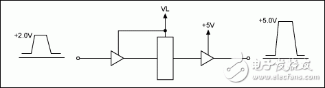
Figure 1. Schematic diagram of line and field signal level shifting
The MAX4885E also provides DDC (display data control) switching, level clamping, and ESD protection. The capacitive load is separated by switching the DDC signal. These signals are compatible with the I2C standard and have a maximum load capacitance of 700pF. If two loads are connected to the same output, the capacitive load may be out of range. The MAX4885E allows only one load to be connected at a time. Similar to other features, the DDC input also has ±15kV ESD protection.
The MAX4885E's DDC switch also provides an additional feature for this type of application: voltage clamping. The DDC voltage from the display is typically pulled up to +5V through a 2.2kΩ resistor (Figure 2). DDC drivers are not allowed to have such high voltages and typically only allow a maximum of +3.3V. The DDC signal is compatible with the I2C standard and has pull-up resistors on both sides of the switch. The switch itself consists of a pair of n-channel transistors.
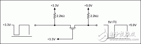
Figure 2. N-channel FET transistor clamp schematic
Due to the effect of the body diode, the n-channel FET can only pass the gate voltage within about 0.7V. When the voltage is close to the gate voltage, the channel resistance increases because the bias voltage is not large enough. When both sides of the switch are pulled up to their respective supply voltages, the n-channel is almost fully clamped. Signals close to ground potential can be transmitted and the switch can be easily pulled down. If the +5V side signal range is: 0.5V to 4.8V, the signal swing on the 3.3V side is 0.5V to 3.3V, as shown above (left side).
in conclusionAs of 2015, analog VGA signals will still be used in mainstream computers, even for longer periods of time. High-definition displays require a signal rise/fall time of less than 1.6ns. In order to achieve such a fast time, the DAC output must maintain the smallest possible capacitance. The MAX4885E VGA switch has a capacitance of less than 7pF and is available in a tiny 4mm &TImes; 4mm package. All outputs of the device feature ±15kV ESD protection, and no additional protection circuitry is required for RGB, line, field outputs, and DDC signals. The MAX4885E also adds a low-to-TTL logic-level converter/buffer that further complements the functional requirements. The line and field signals can be converted from approximately 0.5V to 1.5V to a 5V TTL logic level. The electrostatically protected output is buffered to provide ±8mA drive for the load with a rise/fall time of less than 5ns. In summary, the MAX4885E offers low capacitance switching, clamp protection, and ESD protection. Ideal for notebook docking switches, the MAX4885E provides an evaluation (EV) board for easy device testing and solution evaluation.
What suddenly appear into your mind when hear Mini Gaming PC? Is there quality heat-releasing fan and box design of Mini Gaming PC Build? Does it run stable and smoothly when handle heavier jobs, like Photoshop, Pr, engineering design and drawing, 3d Max, big games, etc. ? now we can be responsible to answer [ Yes". No matter cheap mini gaming pc or Mini Gaming PC Under $500, equips with quality fan to heat releasing. Therefore, no need to worry that again.
To processor, can do from intel celeron j4125, N5105 up to i3, i5 i7 10th 11th 12th with or without video graphics. To slots, same rich as traditional computer tower, like above 4 or 6 usb ports, 2 Rj45, VGA, PD, slot, etc.
You can also find Mini Gaming PC, j4125 Mini PC ,Custom All In One PC, windows 10 Education Laptop,Quad Core Processor Laptop, 15 Inch Gaming Laptop ,windows Yoga Laptop , 8 inch Android Tablet, etc.
If any other special requirements interest, you can also let us know, will try our best support you.
Meet your unique demand in this field is our mission, so just feel free contact us whenever you have different idea.
Mini Gaming PC Build,Cheap Mini Gaming PC,Mini Gaming PC Under $500,Mini Gaming Desktop
Henan Shuyi Electronics Co., Ltd. , https://www.shuyicustomlaptop.com