Abstract: In this paper, a double-diffusion BCD-compatible process based on ultra-thin epitaxial technology is developed for high-voltage energy-saving applications, and a new D-RESURF structure of 700V LDMOS is realized. In the structure, the thickness of the N-type epitaxy is reduced to 4.5 μm, and the length of the drift region is reduced to 70 μm, so that the chip area and the manufacturing cost are greatly reduced. Through the simulation design, the surface electric field distribution of the device structure is optimized, and the reverse breakdown voltage reaches 700V, and the on-resistance of the device is reduced to 33Ω·mm2. The flow sheet results show that the power tube can meet the design requirements.
Key words: ultra-thin epitaxy; D-RESURF; double-well high voltage LDMOS; VLD
0 Introduction SPIC (Smart Power IC) has been widely used in switching power supplies, motor drives, industrial control, automotive electronics, daily lighting, household appliances and other fields. In SPIC, it is often necessary to integrate a high voltage resistant power device with a low voltage control circuit on the same chip. In the field of high-voltage power devices, LDMOS is widely used due to its high operating current density, low on-resistance, and good switching characteristics. From the perspective of process application, LDMOS has the advantage of horizontal structure, and LDMOS, CMOS and BJT devices can be monolithically integrated on the same silicon wafer by BCD process conditions. In the LDMOS design process, the application of new technology determines the withstand voltage and on-resistance characteristics of the device. In this paper, LDMOS maturely introduces D-RESURF technology into the structure. D-RESURF technology introduces a P-type falling field layer on the surface of the N-type drift region to form a node terminal extension region, which can improve the surface electric field and increase The device's reverse breakdown voltage; in addition, D-RESURF technology also increases the density of implantable impurity per unit area of ​​the drift region, thereby reducing the on-resistance of the device.
At present, high-voltage LDMOS generally adopts an epitaxial layer with a thickness of about 10 μm, and its epitaxial thickness is much higher than the current standard CMOS process, and it is required to increase the isolation time for high-voltage integration, and thus is not compatible with standard CMOS processes. In order to solve the above problems, this paper adopts the thin epitaxial layer of P buried layer to perfect the LDMOS structure. In the traditional CMOS process, an LDMOS device with a withstand voltage of 700V or more is simulated on an ultra-thin epitaxial layer with a thickness of 4.5μm.
1 Device Structure and Analysis The dual-diffusion high-power BCD process used in this paper involves many types of devices, including high-voltage LDMOS with a withstand voltage of 700V, medium-voltage MOS transistor with a withstand voltage of 40V, and 5.8V low-voltage CMOS device. , diodes, resistors, etc. Therefore, in the process of designing LDMOS, it is necessary to consider the matching with other devices in terms of process processing, injection concentration, and version.
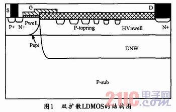
The design requirements of the new double-diffused LDMOS are: under the condition of 4.5μm ultra-thin epitaxial layer, it can meet the high withstand voltage requirement of 700V or higher, and reduce the on-resistance as much as possible; on this basis, compress the drift region length and optimize the device. The structural size is achieved for the purpose of reducing the chip layout area and manufacturing cost. The structure of the double-diffused LDMOS is shown in Figure 1. The multi-ring P-type falling field layer P-topring is divided into several isolated islands to improve the surface electric field of the device. The P-sub in the figure indicates that the P-line is used in the process. Bottom material; LDMOS's withstand voltage drift is divided into two parts:
HVnwel represents the drift region of the N-type epitaxial layer, DNW represents the drift region of the device substrate; Pwell represents the body region of the LDMOS used to form the channel of the MOS device. The LDMOS grid is located above the body region and extends to the right side of the field to form a field plate to improve the electric field distribution on the device surface.
This article refers to the address: http://
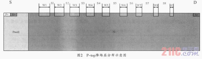
1.1 Structure description of the device surface drop layer The DRESURF technology is used in the design of the device surface drop layer. Multiple P-tops of opposite conductivity types are introduced on the surface of the N-type drift region between the source and drain terminals of the device. Annular doped region. The design of these annular landing layers is based on laterally variable doping (VLD) technology. The VLD technique effectively controls the concentration distribution of the P-top falling field layer on the device surface by changing the size and spacing of the impurity implantation window. After the P-type impurities are implanted at the same implantation concentration, the impurities enter the surface of the drift region through windows of different pitches and sizes, and lateral and longitudinal diffusion are generated at the same ambient temperature, and finally the concentration distribution of the falling field layer on the device surface is approximately linear. A linear increase in concentration from the drain end to the source end allows uniform distribution of the surface electric field. The P-top falling field layer is divided into nine differently spaced regions. As shown in Fig. 2, the lateral dimension Wn of the P-top from left to right is gradually increasing, and the ring spacing Sn is gradually becoming smaller. Approximate linear distribution of P-top falling field concentration from left to right (from leak to source).
The P-type impurities in these P-top regions are implanted in a high-energy, high-concentration manner, which ensures that the device HNV drift region maintains a high impurity concentration to deplete the P-top inversion region in the drift region epitaxial layer. Such a high integrated charge device ensures that the device has a low on-resistance.
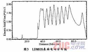
When the device is co-simulated by MEDICI and Tsuprem4 software, the observation results are shown in the electric field distribution diagram of the LDMOS surface. The electric field peaks caused by the high concentration P-top ring in the drift region are evenly distributed in the middle of the electric field in the drift region. The peak values ​​of the electric field waves are similar, about 2×10 15 V/cm. Under this distribution condition, the withstand voltage distribution of the surface electric field of the drift region between the source and the drain of the device is effectively improved.
1.2 Structure Distribution of Device Drift Region The concentration distribution and size structure of the N-type drift region determine the LDMOS electric field distribution and the specific on-resistance. In order to achieve good process compatibility with medium and low voltage MOS, the device drift region is formed by double-well double-injection design method by injecting different doses of N-type impurities into the epitaxial layer and the substrate surface. Before the epitaxial growth, a P-type material is implanted on the surface of the substrate to form a DNW portion of the drift region; after a 4.5 μm thin epitaxial growth, a second implant diffusion is achieved in the ultra-thin epitaxy directly above the DNW to complete the HNV portion of the drift region. . The double injection not only successfully achieves a drift depth of 10 μm on the basis of 4.5 μm ultra-thin epitaxy, but also greatly shortens the drift region length in the lateral direction due to the large increase in the cross-sectional area of ​​the drift region.
In the simulation design process, due to the large dose injection of the P-top falling field layer, the HNV region of the drift region is allowed to maintain a high concentration distribution, and the device has a lower specific resistance than the on-resistance. Since the DNW impurity is reversely expanded in the epitaxial growth heating process and the concentration of the epitaxial layer is increased, the implantation concentration of the DNW region is smaller than HNV. In order to prevent premature breakdown in the body, DNW requires a long time of high temperature heating before epitaxial growth, so that the implanted junction is diffused to the substrate, ensuring that the device maintains a 6 μm drift region junction depth in the longitudinal direction of the substrate. Two different doses and different heating environments are injected to realize the optimal design of the electric field distribution of the device, which effectively meets the technical requirements of the device in different regions.
2 Device simulation optimization design The MEDICI and Tsuprem4 software are used to optimize the device. Under the condition of 4.5μm thin epitaxy, in order to improve the surface electric field of the device and make the device with the highest withstand voltage greater than 700V, the P-top implant dose and structure size were simulated and optimized. At the same time, the influence of drift region concentration on breakdown voltage and on-resistance is analyzed, and the optimal concentration distribution range is obtained through simulation.
2.1 Simulation optimization of P-top implant dose and structure size Since the junction depth of the P-top field in the longitudinal direction is very shallow, the concentration change is negligible. Here, the one-dimensional model of the P-top falling field layer along the x direction is mainly analyzed. The impurity concentration distribution of the multi-ring injection is R(x, t), Cfo(x, t) and Cfi(x, t) are respectively The impurity concentration distribution of the first ring and the i-th ring after the junction time (T) is: 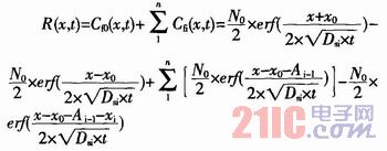
The window size and spacing of the P-top ring in the layout can be adjusted by the formula to achieve linear doping of the P-top falling field layer. Considering the level of process fabrication and error, in order to avoid process distortion, the size and spacing of the window are not too small, but if the spacing of the window is too large, it is not easy to achieve linear doping of the falling field layer. Therefore, it is necessary to select a suitable window. Size and spacing. After the simulation design and actual test, two sets of specific window sizes are obtained, as shown in Table 1.
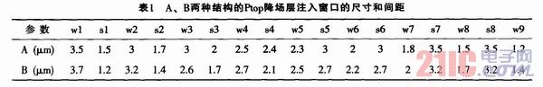
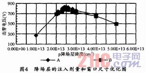
The injection dose and window size of the P-top falling field layer are optimized. The simulation results are shown in Fig. 4. When the window size is small (A structure) is more linearly doped, the concentration is 2. In the range of 2E13cm-3~3E13cm-3, the breakdown voltage of the device is more than 700V, and the injection dose of the B structure with larger window size is only in the range of 2.3E13cm-3~2.8E13cm-3, which meets the device breakdown voltage greater than 700V, obviously the range of variation is small, and the complexity of the process is improved. Therefore, the optimum value of 2.5E13cm-3 in the A structure is selected here for process design.
2.2 Influence of drift region concentration on breakdown voltage and on-resistance When the drain terminal potential increases from zero to about 220V, the intrinsic PN section depletion region expands with the increase of voltage until the entire drift region is completely consumed. At this time (the peak electric field of the PN section in the body is much smaller than the minimum value of the breakdown electric field), the P-top, N-junction on the surface of the device and the N- and P-sub junctions in the device body continue to increase during the voltage increase. The peak of the electric field rises accordingly. Under the condition that the total implantation dose of the N-type drift region is constant, the increase of the HNV injection dose causes the breakdown point of the electric field on the surface of the LDMOS to be shifted from the drain end to the source end of the P-top. When the HNV injection dose is 1.1E 12cm-2~1.35E12cm-2, the concentration of the N-type drift region is low, and the drift region of the LDMOS is completely depleted at a low drain-source voltage, and the electric field is concentrated in the drain region. The device first breaks down in the drain/N-type drift region; the increase of the impurity concentration on the surface of the N-type drift region causes the P-top to be completely depleted, the surface electric field distribution is more uniform, and the on-resistance tends to decrease. When the HNV injection continues to rise, when the concentration of the N-type drift region is too high, the drift region of the LDMOS cannot be completely depleted, and the electric field is concentrated on the side of the source region of the P-top falling field layer, and the device also prematurely breaks down. At the same time, the implantation concentration of DNW is gradually decreasing, so that the overall drift region will gradually increase in on-resistance. Therefore, it is necessary to compromise the influence of the N-type drift region concentration on the breakdown voltage and the on-resistance of the device.
TSUPREM4 and MEDICI simulate the drift region concentration distribution. When the total implant dose in the drift region is in the range of 2.4E12cm-2~2.7E12cm-2, the HNV keeps the implant dose at 1.1E12cm-2~1.8E12cm-2. The device breakdown voltage is greater than 700V. Considering the factors such as process error, the total implant dose in the drift region is selected as 2.5E12cm-2 and 2.6E12cm-2, respectively. When the HNV implant dose is changed from 1.1E12cm-2 to 1.8E12cm-2, the breakdown voltage is observed and analyzed. The variation of BV and on-resistance Ron is shown in Figures 6 and 7.
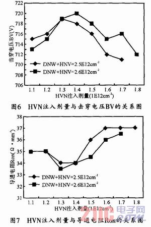
Observing the relationship between the HVN implant dose and the breakdown voltage BV and the on-resistance Ron, when the HNV implant dose is increased by 1.1E12cm-2, the surface concentration of the device is improved, the breakdown voltage is increased, and the on-resistance is correspondingly Decreasing, as the concentration increases, the device drift region concentration distribution tends to be optimized. When the HNV injection dose continues to increase beyond 1.5E12 cm-2, the surface concentration of the drift region is excessive, and the device breaks down near the falling field layer at this time. The breakdown voltage is gradually reduced. At the same time, the implantation of the drift region DNW gradually decreases with the increase of HNV, and the concentration distribution of the device drift region is unbalanced, resulting in an increase in the on-resistance of the device. Therefore, when the HNV injection dose is 1.3E12cm-2~1.5E12cm-2, the DNW injection dose is 1.1E12 cm-2~1.3E12cm-2. At this time, the on-resistance of the corresponding simulation result is less than 35 Ω·cm 2 , and the breakdown voltage BV is greater than 714V.
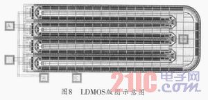
3 Conclusion This paper designs a dual-well LDMOS based on ultra-thin epitaxial technology. The new device uses D-RESURF, laterally doped (VLD), double-well injection drift region and other technologies. The HNV injection concentration and breakdown voltage were studied by simulating the geometry and implant concentration of the drift field surface to improve the withstand voltage characteristics of the device surface. At the same time, the total implant dose in the drift region was constant. The relationship between the on-resistance and the on-resistance is analyzed to obtain the optimal concentration distribution. According to the results of these simulation designs, the LDMOS is tested and the device layout is shown in Figure 8. When the P-top injection dose was 2.5E13 cm-3, the HNV injection dose was 1.3E12 cm-2. When the DNW injection dose is 1.3E12cm-2, the test device results show that the LDMOS breakdown voltage can reach 690V, and the result is close to the design requirements, achieving good process compatibility with medium and low voltage devices.
The Preformed Helical Fitting is mainly used in wire,ground wire installed hardware. According to the performance of the structure can be divided into:
1.Preformed Suspension Clamp:used to hang the conductors and ground wires on the perch.
2.Preformed Strain Clamp:bears all tension,connect the wire and ground wire on the tension tower
3.Splicing Fitting:used to two ends of conductor,instead of the conventional hydraulic compression splicing sleeve and pressure pipe.
4.portective fitting:used to protect the conductors and insulators,generally divided into armor rod,repair sleeve,vibration damper.
Material generally adopt aluminum alloy,hot-dip galvanized steel. Fasteners are hot-dip galvanized steel.

Preformed Helical Fitting
Preformed Helical Fitting,Preformed Splicing Fitting,Preformed Protective Fitting,Preformed Line Fitting
Jiangsu Chuandu Electrical Technology Co.,Ltd. , http://www.cdepf.com