1 Introduction
White LED is considered to be a “green lighting source†because of its high efficiency, low power consumption, long life, solid-state energy saving, and environmental protection. It is expected to become the third generation of illumination source after incandescent and fluorescent lamps. Development potential. The use of phosphor conversion to achieve white light is currently the most researched and hottest method. At present, the power-type white LED packaging process is still immature, and the heat dissipation and phosphor coating are the key breakthroughs of the two packaging processes. For white light power LEDs used in the field of illumination, the uniformity of spatial distribution of color temperature and chromaticity is an important indicator of product performance. The color temperature difference that can be distinguished by the human eye is 50-100 K. At present, the uniformity of the chromaticity of ordinary LED devices is still not ideal, and even the angular color temperature difference of a single LED can be as large as 800 K. This is because when the concentration of the phosphor is constant, the probability of blue light being converted into yellow light is proportional to the thickness of the phosphor encountered during the blue light emission. The uneven thickness of the phosphor is the main cause of the difference in the angular color temperature of the white light LED. It can be seen that for white LEDs, research and improvement of white spot uniformity is an important issue.
2 sample making process
We use the current mainstream potting and dispensing process, using different phosphor layer shapes and structures, and made five kinds of samples, A1 ~ A5. The phosphor layer is mainly processed in two steps. First, a chip is coated on the chip. A layer of transparent silica gel is dried to form a transparent silica gel layer; a mixture of phosphor and transparent silica gel is applied to the silica gel layer. Figure 1 (a ~ e) is a schematic diagram of five different shapes of structured white LEDs. On the front side of the chip, the phosphor layer has a thickness of about 25 μm.
As shown in Fig. 1(a), the structure of the sample A1 is first coated with a thicker silica gel layer on the light-emitting layer of the LED chip, which is about twice as thick as the phosphor layer, and the silica gel layer covers the substrate base of the entire metal. The seat is coated with a phosphor layer on the dried silica gel layer. As shown in Fig. 1(b), the structure of the sample A2 is basically similar to that of the A1 structure, and a silica gel layer is applied on the light-emitting layer of the LED chip, and the thickness thereof is about 1 /2 of the phosphor layer, and the silica gel layer covers the entire metal. The substrate pedestal is then coated with a phosphor layer, which is slightly different in that the thickness of the silica gel layer is significantly thinner at this time, but the error may be large due to manual operation. As shown in FIG. 1(c), the sample A3 has a structure in which a silica gel layer is coated on the metal base along the edge of the substrate, and the height of the silica gel layer does not exceed the ceramic substrate of the flip chip, and is filled with the ceramic substrate. The luminescent layer on the chip has no silica gel, and after drying, a phosphor layer is coated on the entire chip. As shown in FIG. 1(d), the sample A4 has a structure in which a silica gel layer is coated on the metal base and the ceramic substrate along the edge of the light emitting layer of the chip, and the height of the silicone layer does not exceed the center of the chip of the flip chip, just like The luminescent layer of the chip is filled in, the upper surface of the luminescent layer is exposed, and after drying, a phosphor layer is coated on the entire chip. As shown in Fig. 1(e), the sample A5 has a structure in which a silica gel is applied to the front surface of the light-emitting surface of the chip, the thickness of which is the same as that of the phosphor layer, and then a phosphor layer is applied on the dried silica gel layer.
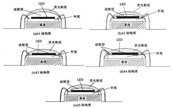
Figure 1 Schematic diagram of the process of making five white LEDs
3 Establishment of experimental test platform
The 9-point color coordinates and color temperature of each LED were tested by a 9-point method to determine the spatial uniformity of illumination in each direction of a single LED exit spot. The color temperature and chromaticity of the device were tested by the integrating sphere method to investigate the difference between the devices of the same type of sample.
In order to test the spatial uniformity of the exit spot of a single white LED, the following experimental platform was established: the test was carried out in a dark room to reduce the effects of ambient light. First fix the LED on the wall, and place a white screen directly in front of it. The height of the center of the screen is the same as the LED (as shown in Figure 2). The screen and the wall are parallel. In order to facilitate the test and statistics, we selected 9 points that form a square as a representative measurement point.
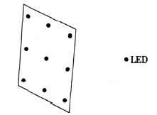
Figure 2 Test screen and LED position diagram
Experimental conditions: The 1W white LED is fabricated in this paper. It is driven by a 350mA constant current power supply with a voltage of about 3.5V. The distance from the LED to the screen is the same, 60cm. The tools used for the test are: CHROMA METER CS2100M INOLTA color difference meter. Measurement of luminous flux, color temperature and color coordinates of a single device; the ssp3112LED spectral wavelength analysis system used to measure the chromaticity coordinates and color temperature of the entire LED using the integrating sphere method. The dispersion of chromaticity coordinates can be expressed by the standard deviation of the chromaticity coordinates of the nine test points of each LED. Let the color coordinates of the nine test points be ( xi , yi ) ( i = 1, 2, ⋯, 9 ), the average of the color coordinates of the 9 test points is  , the standard deviation is σ:
The dominant wavelength distribution also reflects the 9-point color coordinate dispersion. The smaller the dominant wavelength range, the more concentrated the 9-point color coordinates, the more uniform the spatial chromaticity distribution of the LED. In addition, the color deviation of this LED illumination can be seen from the magnitude of the dominant wavelength. The dominant wavelength is mainly represented by the mapping method.
The chromaticity uniformity between the devices can be expressed by the standard deviation of the chromaticity coordinates and the standard deviation of the color temperature, and can also be directly reflected by the distribution on the CIE1931 chromaticity diagram. Let the color coordinates of the device obtained by the test be ( xi , yi ) ( i is the number of devices), the average color coordinate of a batch of devices is ( x, y ), and the standard deviation of the chromaticity coordinate points is:
The standard deviation of the color temperature is:
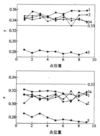
Figure 3 9-point color coordinate distribution of sample space
4 test data and discussion
4. 1 Single LED white spot uniformity
In order to investigate the optical consistency of the exit spot of a single white LED, a sample is randomly selected from the samples A1 to A5, and the spatial distribution of the color coordinates of each LED is measured by the 9-point method, and the standard of the color coordinates is calculated according to the formula. The difference σ and the dominant wavelength distribution are shown in Table 1. The spatial 9-point chromaticity coordinate values ​​of the individual white LEDs of each sample in Table 1, ie, the (x, y) values, are plotted on the line graph 3 to examine the dispersion, as shown in the figure, x = 0.33, y = The 0.33 point is the ideal white spot. The 9-point chromaticity coordinate position of the A1~A5 sample is plotted on the C IE1931 chromaticity diagram 4 to more intuitively reflect the spatial distribution of the chromaticity, and the main wavelength distribution area is marked, and the samples of A1~A4 are included. The chromaticity distribution is embedded in the thumbnail.
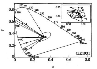
Fig.4 CIE1931 chromaticity diagram of 9 points in sample space A1~A5 and its main wavelength range distribution

Table 1 Standard deviation and dominant wavelength distribution of 9-point color coordinates of samples A1 to A5
In order to analyze the simplicity and grasp the main contradiction of the problem, we ignore the influence of the uneven illumination of the chip itself and the error of manual operation in the analysis process. Only the effect of the process on the uniformity of the illumination is considered. It can be seen from the above table and figure that the standard deviation of the color coordinate of A3 process is relatively small. From the line graph and the chromaticity diagram, the 9-point color coordinate distribution is more concentrated, and the main wavelength range distribution is also smaller. The process can be better controlled. The uniformity of the thickness of the phosphor makes the exit spot more uniform and the emitted light is also close to the standard white light. A4 is slightly behind A3. The uniformity of A1 and A2 is not good and the dispersion is greater. A5 can improve uniformity, but it is too far from ideal white light and has poor control over thickness.
Since A3 employs a process in which a layer of silica gel is applied to the metal pedestal along the edge of the substrate to fill it with the ceramic substrate, this results in a more uniform distribution of the phosphor layer over the luminescent layer of the chip. Because the silica gel fills the ceramic substrate, the thick phosphor layer on the side is thinned, and the bottom area is increased, so that the plane of the phosphor layer distribution is increased, so that the phosphor layer is formed on the chip to be flatter. It also makes the phosphor layer evener. The structure of A4 is along the edge of the light-emitting layer of the chip, so that the silica gel layer fills the light-emitting layer on the surface of the chip, which can increase the flat area on the chip and improve the uniformity. However, since the light-emitting surface also emits light beside the surface of the chip, the first layer of silica gel is applied on the side, which causes blue light to be emitted next to it, and the process operation is worse. The A5 structure is first coated with silica gel on the chip, which first forms an arc shape. In principle, the arc difference of the phosphor layer can be reduced, so that the phosphor layer is more uniform on the chip, but it is because of the underlying silica layer. The amount of phosphor is reduced, causing A5's luminescence to shift to blue light, and because the chip is smaller, the operation is more difficult and the controllability is worse. The structures of the samples A1 and A2 are basically similar, and a silica gel layer is first applied on the light-emitting layer of the LED chip, which basically does not change the shape of the phosphor layer on the chip, and certainly does not improve the uniformity of the phosphor layer.