567 is a universal tone decoder that provides a saturated transistor-to-ground switch when the input signal is in the pass band. The circuit is composed of an I and Q detector, and the voltage controlled oscillator drives the oscillator to determine the center frequency of the decoder. The center frequency bandwidth and output delay are independently set with external components.
This article refers to the address: http://
Mainly used for oscillation, modulation, demodulation, and remote control coding and decoding circuits. Such as power line carrier communication, walkie-talkie sub-audio decoding, remote control and so on. 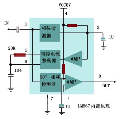

With an external resistor 20 to 1 frequency range logic compatible output has a current absorption capacity of 100mA.
Adjustable bandwidth from 0% to 14%
Wide signal output and high noise rejection for false signal anti-jamming high stability center frequency center frequency adjustment from 0.01Hz to 500kHz
The power supply voltage is 5V--15V, 8V is recommended.
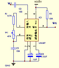
Application example: Input terminal 104 capacitor, output terminal pull-up resistor 10K, C1, C2 is 1uF. R1 and C1 determine the oscillation frequency. Generally, C1 is 104 capacitors, and R1 is 10K-200K. The power supply voltage is 8V.
Single channel infrared remote control circuit
In applications where multiplex control is not required, a single channel infrared remote control circuit consisting of conventional integrated circuits can be used. This remote control circuit does not require the use of a more expensive dedicated codec and is therefore less expensive.
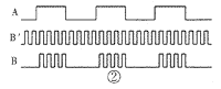
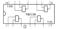
The single channel infrared remote control transmitting circuit is shown in Figure 1. A high speed CMOS type quadruple two-input NAND gate 74HC00 is used in the transmit circuit. The NAND gates 3 and 4 form a carrier oscillator, and the oscillation frequency f0 is adjusted to about 38 kHz; the NAND gates 1 and 2 constitute a low frequency oscillator, and the oscillation frequency f1 does not have to be precisely adjusted. F1 modulates f0, so the waveform output from the NAND gate 4 is an intermittent carrier, which is also the waveform transmitted by the infrared light emitting diode. The waveforms of several key points are shown in Fig. 2. In the figure, the waveform of B' is the waveform outputted by point B when the point A is not added with the modulation waveform and is directly connected to the high level. It can be seen from FIG. 2 that when the waveform of point A is high level, the infrared light emitting diode transmits a carrier; when the waveform of point A is low level, the infrared light emitting diode does not transmit a carrier. The frequency of this stop is the low frequency oscillator frequency f1. Why not use the low-speed CMOS quad-two-input NAND NAND CD4011 in the infrared transmitting circuit, and use the higher-priced 74HC00? Mainly due to the limitation of the power supply voltage. The infrared emitter has a variety of housings, but the power supply is typically designed to be 3V, using two 5 or 7 batteries for power. Although the CD4011's nominal operating voltage is 3 to 18V, it is for processing digital signals. Because the CMOS NAND gate is used for oscillating to generate a square wave signal, that is, an analog application, its operating voltage is at least 4.5V, otherwise it is not easy to start and affect the use. The 74HC series CMOS digital ICs have a minimum operating voltage of 2V, so using a 3V power supply is “handyâ€. The pin function of the 74HC00 is shown in Figure 3. 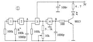
Â
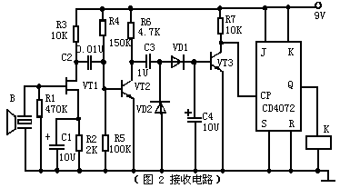
4 is an infrared receiving demodulation control circuit. In the figure, IC1 is LM567. The LM567 is a phase-locked loop circuit with an 8-pin dual in-line plastic seal. The external resistors and capacitors of pins 5 and 6 determine the center frequency f2 of the internal voltage controlled oscillator, f2≈1/1.1RC. Its 1 and 2 pins are usually grounded through a capacitor to form an output filter network and a loop single-stage low-pass filter network. The capacitance of the 2 pin determines the capture bandwidth of the phase-locked loop: the larger the capacitance, the narrower the loop bandwidth. The capacity of the capacitor connected to the 1 pin should be at least 2 times the capacitance of the 2 pin. Pin 3 is the input and requires an input signal ≥25mV. Pin 8 is the logic output and internally has an open collector transistor that allows a maximum sink current of 100mA. The LM567 operates from 4.75 to 9V, operates from DC to 500kHz, and has a quiescent operating current of approximately 8mA. The internal circuit and detailed working process of the LM567 are very complicated. Here, only the basic functions are summarized as follows: When the LM567's 3-pin input amplitude is ≥25mV and the frequency is within its bandwidth, the 8-pin changes from high to low. The 2 pin outputs a modulated signal with frequency/voltage conversion; if an audio signal is input at the 2 pin of the device, the FM square wave signal modulated by the 2-pin input modulation signal is output at the 5 pin. In the circuit of Figure 4, we only use the LM567 to receive the carrier signal of the same frequency and the voltage of the 8-pin voltage from high to low to form the control object. 
Ultrasonic remote control fan transmission <br> I. Working principle
(Fig. 3) is a transmitting circuit. It uses the remote control transmitter of the domestic bat brand FS-A5A Electric Fan. The transmitter has the characteristics of small size, low power consumption, reliable operation, and simple circuit. In use, each time the launch button is pressed, the transmitter emits a 40 kHz ultrasonic wave of approximately 500 ms. The working principle of the transmitting circuit is as follows. 
VT2 and VT3 form a direct coupled positive feedback oscillating circuit, B is a 40KHz ultrasonic transmitting device, and the oscillating circuit feeds back the pre-frequency components. Therefore, this circuit can accurately oscillate at the center frequency of the ultrasonic transmitting device of 40 kHz. VT1 and R2, C1 form a 500ms delay circuit. R1 and VD1 are the discharge paths of C1. When the emission key S is pressed, the oscillation circuit formed by VT2 operates to emit ultrasonic waves, and at the same time, the power supply charges C1 through R2, when the potential on C1 is charged to 1.4V (about 500 ms). ), VT1 is turned on, VT2 base and VT3 collector potential drop is about 0.3V, the oscillator stops working. When the emission key S is released, C1 is quickly discharged through VD1 and R1, ready for the next launch. VD3 And R4 constitutes a transmission indicating circuit, and when the transmitting key is pressed, VD3 emits light.
(Fig. 4) is a receiving circuit. The CMOS non-gates D1~D3 are biased by R1 to be linear amplifiers with a total gain of more than 60bB. Due to the high input impedance of the CMOS circuit, it is well matched to the ultrasonic receiving device. The amplified signal is coupled by C1 to the input pin 3 of the phase locked loop decoder LM567. When the frequency of the input signal falls on its center frequency, the logic output terminal 8 of the LM567 changes from high level to low level.   
 
Frequency selective voice switch <br> This voice control switch can control the opening or closing of any appliance by a specific tone (500 to 2000 Hz) sound. Because it has a certain frequency selection effect, the probability of malfunction is small.
The circuit is designed to be controlled by an audio electrical signal (up to 100 mV), and the control signal source can be a telephone, a radio, a record player, a recorder, and a shielded wire is taken from the appropriate point. If you want to use sound wave remote control, add an electret microphone and a level of preamplification.
The circuit of this device is shown in Figure 16. Its central device is a pickup integrated circuit LM567, and a 50mA relay.
After a certain tone audio signal is added to the input end (3 feet) of the LM567, it is processed by the internal circuit for amplification, frequency selection, etc., and outputs a low level at the output terminal 8 (high level when there is no input signal). At this time, a PNP tube (2N3906) connected thereto is turned on, so that the relay connected in the collector circuit is sucked, thereby controlling the controlled device with its contact. If it is used to start up, it will use the normally open and movable contact of the relay; if it is used for shutdown, it should use the common and open contact.
The response frequency is determined by the value of the potentiometer and capacitor connected to pins 5 and 6, so adjust the 10kΩ potentiometer to adjust its response frequency. The range of audio that can be received by this unit is 500 to 2000 Hz.
Diode 1N4001 is used to protect the transistor. 2N3906 can be replaced by any other type of medium and low power PNP silicon tube. 
After clarifying the basic working principle and function of the LM567, it is very simple to analyze the circuit of Figure 4. IC1 is an infrared receiving head, which receives the infrared signal emitted by the transmitter, and its center frequency is the same as the transmitter carrier frequency f0. After demodulation by IC1, the square wave signal with the frequency f1 is outputted at the output terminal OUT, that is, with FIG. The signal with the same waveform at point A. We adjust the center frequency of the LM567 to the same frequency as the NAND gates 1, 2 in the transmitter, even if f2 = f1. Then, when the transmitter transmits a signal, the LM567 starts to work, and the 8 pin changes from a high level to a low level. With this varying level, various objects can be controlled. Using the circuit of Figure 4, we can make a remote control switch to remotely control various household appliances in the home.
In fact, using the circuit shown in Figures 1 and 4, we can also easily transform it into a multi-channel remote control circuit. The method is: in the transmitter (Fig. 1), the resistance R* is changed into several different values, thereby forming several kinds of modulation signals with different frequencies; in the receiving circuit, several LM567 are set, and the inputs are all from the infrared receiving Head, each LM567 has a different oscillation frequency but one-to-one correspondence with the transmitting end. Thus, when the transmitter presses a different button and accesses a different modulation signal, the level of the 8-pin of the LM567 corresponding to the receiving end changes, thereby forming a multi-channel control. Strictly speaking, this is a kind of frequency division multiplexing. Compared with digital codec multi-channel control, the disadvantage is that debugging is more complicated. But in some occasions, such as in multi-channel alarms, there is also a place. In the alarm application, when it is necessary to solve the problem of two or more simultaneous alarms, there is a complicated synchronization problem with time division multiplexing, and it is easy to solve with frequency division multiplexing when the bandwidth is allowed.
Ultrasonic remote control circuit
1, ultrasonic remote control light switch <br> This remote control switch, the circuit is simple, and free of debugging, very suitable for beginners.
First, the working principle is the transmitting circuit. The circuit is composed of discrete devices. VT1 and VT2 and R1~R4, C1 and C2 form a self-excited multivibrator. The ultrasonic transmitting device B is connected in the collector loop of VT1 and VT2, and works in push-pull mode. Determined by R1, C1 and R4, C2. The resonant frequency of the ultrasonic transmitting device B causes the multi-resonant circuit to trigger. Therefore, this circuit can operate at the optimum frequency. 
(Fig. 2) is the receiving circuit. The junction field effect VT1 constitutes a high input impedance amplifier, which can be well matched with the ultrasonic receiving device B, and can obtain higher receiving sensitivity and frequency selective characteristics. VT1 adopts self-biased bias mode. When R3 is changed, the operating point of VT1 can be changed. Ultrasonic receiving device B converts the received ultrasonic wave into corresponding electric signal, and after being amplified by VT1 and VT2, half-wave is transmitted through VD1 and VD2. The rectification becomes a DC signal, which is integrated by C3 and acts on VT3 and the base, so that VT3 changes from off to on, its collector outputs a negative pulse, and the trigger JK triggers D to flip it. The level of the Q terminal of the JK flip-flop directly drives the relay K to cause K to pull or release. The switch of the circuit is controlled by the contact of the relay K.
Second, the component selection <br> In the transmitting circuit, VT1 and VT2 use small power transistors such as CS9013 or CS9014, ≥100. The ultrasonic transmitting device uses SE05-40T, and the power supply GB uses a 9V laminated battery to reduce the volume and weight of the transmitter.
In the receiving circuit, VT1 and 3DJ6 or small power junction field effect transistors such as 3DJ7. VT2~ VT3 uses CS9013, ≥100. IN4148 is used for VD1 and VD2. JK flip-flop 263B. The ultrasonic receiving device is paired with SE05-40T with SE05-40R. Relay K uses the HG4310 type.
Electric Fan is a home appliance driven by an electric motor through the blades rotary, promote air accelerate circulation, mainly used to cool the hot weather and circulation of air. The electric fan is easy to install, dismantle and move. Electric fan is widely used in homes and public places. Our factory produce and sale stand electric fan, wall electric fan, table electric fan and bladeless electric fan, etc. Our electric fan`s pure copper motor with high quality reinforced Silicon steel sheet and new enameled wire, higher magnetic permeability, less power attenuation, more power, more stability, longer life, more energy-saving; The electric fan`s motor optimization technology applied, motor temp rise less than 65k when full loading, with over heat protection, more safety; The electric fan`s blades adopt new AS material, more stablility, more power, more wind, no deformation, no broken, anti-aging.
Electric Stand Fan, Portable Electric Fans, Wall Mount Electric Fans, Industrial Electric Fan
Ningbo APG Machine(appliance)Co.,Ltd , http://www.apgelectrical.com