Abstract: In order to solve some problems in the standard definition monitoring system, a high-definition video compression system based on TMS320DM365 is designed. Adopting ITU-T H. 264 (DM365 embedded hardware compressor) video compression algorithm, high-definition analog video signal is converted into digital video signal by dedicated video decoding chip TVP7002, data compression in DM365, embedded ARM data is packaged and transmitted to the internet, through PC Software decoding for video playback. Practice has proved that this coding scheme has completed the data compression and transmission well and meets the design requirements.
Keywords: video compression; DM365; H. 264; network transmission
In video surveillance applications, traditional video surveillance has a high image clarity (CIF to D1 resolution), difficulty in managing and maintaining many cables, complicated configuration of many devices, and inconvenient expansion. These factors seriously restrict the security management effectiveness. Enhancement, but also brings an opportunity for the development of high-definition video surveillance, this paper discusses the hardware design of HD video encoder based on DM365.
1 Hardware platform overall design TMS320DM365 continues the architecture of the DavinciTM family DM355 processor, integrating an ARM926EJ-S core, an image processing subsystem (VPSS), an H. 264 HD encoder coprocessor HDVICP and an MPEG-4/JPEG HD encoder coprocessor MJCP, support multi-format H. 264, MPEG-4, MPEG-2, MJPEG, and VC1 codecs for high video flexibility. DM365 can simultaneously output 720P, D1, CIF three streams, or more combinations, and the encoding rate is adjustable, and supports hardware OSD. The processor has a rich peripheral interface, and the user can conveniently connect the subsystem. This paper adopts TMS320DM365 as the main CPU, collects the input video data and performs corresponding compression network transmission processing, and designs a digital video encoder based on DM365 architecture. In addition to DM365, the system also has high-definition video A/D converter, audio CODEC, storage, Ethernet, serial port and other modules. The system runs on the Linux operating system and has the characteristics of good real-time performance, fast communication speed, high image quality, stable performance, low price and anti-virus.
The overall block diagram of the system is shown in Figure 1. The system uses DM365 as the main CPU, DM365 external audio module, video input module, storage module, serial port and network transmission module. The platform consists of two parts: the video input and image processing part and the video output part.
This article refers to the address: http://
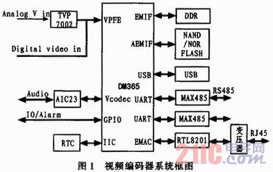
Video input and image processing part: High-definition analog video signal input TVP7002, after A/D encoding, it becomes high-definition digital video signal, and this digital signal is output to DM365. This module DM365 mainly performs H. 264 compression, and can achieve noise filtering, video stabilization, face detection, auto white balance, auto focus, auto exposure and edge enhancement. In addition, it also initializes all I2C devices on the system to implement audio and voice intercom.
Video output part: DM365 embedded ARM microprocessor, the core function of this processor is to forward data stream, external memory module, Ethernet module, serial port module, etc. ARM first completes the RTP, UDP, and IP encapsulation of the compressed data, and then passes through the MAC framing, and finally completes the transmission of the data packet through the Ethernet controller PHY. In addition, ARM is also responsible for parsing the received data, forwarding the relevant parameter commands sent by the PC, performing corresponding operation settings (video compression rate, frame rate, etc.), and implementing peripheral control through the serial port (pTZ controller, lens) Etc.), the processing of alarm input and output through GPIO, and so on.
2 module design
2.1 Video Audio Input Module There is a VPFE interface on the DM365, which can support video input formats in multiple formats. The system realizes 1 channel HD video input, and the HD A/D conversion chip adopts TVP7002. The TVP7002 can realize digital conversion of R/Pr, C/Y, B/Pb signals with a conversion rate of up to 165 MHz. It is used in many high-definition digital video environments with a resolution of up to 1080P. The DM365 is configured through the IIC bus. The TVP7002 internal registers are properly configured to process 720P resolution video sources. The A/D video data is output from the TVP7002 digital video port to the DM365 VPFE. The system also provides high-definition digital video input interface, HDVICP coprocessor can provide H in 1 280X720P30 format. The 264 standard video encoding or decoding, and the MJCP coprocessor in addition to the JPEG standard, can also provide MPEG-4 video encoding or decoding in the 1 920x1 080P24 format.
The system realizes one LINEIN and stereo output through AIC23, DM365 is configured through IIC bus, and AIC23 is connected to MCBSP port of DM365. The MCBSP of the DM365 is used as a bidirectional data channel through which all audio data streams are transmitted and supports different data formats.
2.2 Ethernet Module The system includes an I-channel 10/100M network interface, the DM365 has a MAC controller, and an Ethernet PHY chip is connected to the EMAC interface. The PHY uses RTL8201, and the RTL8201 is connected to the MII interface of the DM365. The DM365 implements the configuration and control of the RTL8201 register through the MDIO interface. The other handshake signals are sequentially connected. The RTL8201 is properly configured (set the PHY address, etc.) by pulling up and pulling the pull-down resistor. The RTL8201 imports these configuration information at the beginning of power-on and performs corresponding work. An external 25 MHz crystal is connected to the clock interface of the RTL8201 as the clock source for the RTL8201. The RTL8201 is connected to a network transformer for signal isolation and is connected to the network via RJ45.
2.3 Storage, USB, serial port, RTC, alarm module system provides 1 channel USB interface, supports OTG mode and HOST mode, supports USB2.0 High Speed ​​(480 Mb/s), Full Speed ​​(12 Mb/s), Set the FIFO. The DM36 5 on-chip USB Controler and USB PHY complete its initialization through related configuration, and external peripherals such as USB-SATA hard disk can be connected to the USB.
The system externally connects DDR2 SDRAM and NAND Flash as off-chip memory. The boot mode is NANDFlash BOOT mode by setting BTSEL[2:0] to 000. DM365's AEMIF interface can support NANDFlash and NOR Flash. Because NAND Flash has large storage capacity and low price, this design uses NAND Flash.
DM365 provides a dedicated DDR2 control interface, 16-bit data line, 14-bit address line and 3 block selection signals, which can support 256 MByte of storage space. The system uses DDR2 SDRAM chip K4T1G164QQ.
DM365 has 2 UART interfaces, the system is connected with two serial ports, one RS232, used for debugging, and one RS485 peripheral for communication (PTZ lens, etc.). And through GPIO to provide 2 way switch alarm input and 2 way switch alarm output, the alarm input is realized by the diaphragm. When the alarm signal is input, the light is turned on, and the output is low to DM365 GPIO, when there is no alarm signal input. When the aperture is cut off and the output is high to DM365 GPIO, the DM365 determines the presence or absence of the alarm input signal by detecting the GPIO level. The alarm output is realized by controlling the opening and closing of the relay. The system also extended the RTC through the IIC.
The system provides a 24 MHz clock input to the DM365 via an external crystal and a module clock from the DM365 internal PLL.
2.4 Power Supply The system provides a 5 V power input interface that provides +1.35 V, +1.8 V, and +3.3 V power through the power conversion chip. Among them, 1.35 V and 1.8 V are generated by TPS62040DGQ. The TPS62040DGQ is a high efficiency, low ripple DC-DC chip from TI that regulates the output voltage through a resistor. The 3.3 V voltage is implemented with the TPS5430, which has a maximum input voltage of 36 V and a maximum current of 3 A.
The power-up sequence for the system is: first power up the core (1.35V), then power up the PLL and other modules (1.8V). That is, the 3.3V power supply is first obtained through the TPS5430, then 1.35 V is generated by the TPS62040DGQ, and 1.8 V is connected to the EN of another TPS62040DGQ through 1.35 V. After 1.8 V is generated, the current is turned on through the switch. The resulting 3.3 V, 3.3 V is finally loaded onto the DM365. The order in which the power is generated is opposite to the power-on sequence.
3 Conclusion In order to test whether the design meets the predetermined requirements, the system performance has been tested thoroughly. A variety of high-definition video input sources have been selected for testing in different environments. There are tests for the speed and severity of the test. The black and white of the image effect, as well as the step pattern for testing the brightness level.
The experimental results show that the system can encode in real time, the decoded image is clear and smooth, there is no mosaic and animation phenomenon, no overexposure, lack of portrait exposure, color cast, exposure and white balance inaccuracy, etc., with bright colors and clear brightness. Overcome the shortcomings in the standard definition monitoring system.
This design solution is economical to use, in line with the original intention of design, and has broad market prospects in the fields of videophone, high-definition monitoring system and vehicle monitoring.
Full Body Screen Protector,Full Coverage Screen Protector,Invisible Tpu Screen Protector,Smooth Screen Protector
Guangzhou Ehang Electronic Co., Ltd. , https://www.ehangmobile.com