The purpose and significance of the research
The spectrum analyzer can help the designer to determine the frequency range of the interference signal in order to select a reasonable filtering scheme. However, the general spectrum analyzer is large in size and is not convenient for industrial use. Therefore, the handheld spectrum analyzer is designed to be portable and power-consuming. Low, can record data for a long time, and can be operated remotely through the network.
The design of the spectrum analyzer is based on the Xilinx FPGA. The analog amplifier is used to drive the programmable amplifier to complete the amplification and level shifting of the analog signal. Then, the ADC is driven to complete the data acquisition according to the set sampling frequency, and then the fast Fourier is completed. Transform, and finally display the result on a 4-inch color LCD screen and store the data according to the settings or transfer data through the network.
Spectrum analysis has a wide range of applications in production practice and scientific research. The so-called spectrum analysis is to spread the signal strength of the signal source in frequency order, making it a function of frequency, and examining the law of change. For the study of an electrical signal, we can analyze its characteristics over time, or it can be described by the frequency components it contains (ie, the spectral distribution). The former is often referred to as time domain analysis, and the latter is referred to as frequency domain analysis of signals. By performing spectrum analysis on the signal, the frequency structure of the signal can be obtained to understand the frequency component of the signal or the characteristics of the system. On this basis, the tracking control of the signal can be realized, thereby realizing the early prediction of the system state, discovering the potential danger and diagnosing the cause of the failure, and identifying and correcting the system parameters. Therefore, spectrum analysis is an important method to reveal signal characteristics and an important means of processing signals. The instrument for spectrum analysis is a spectrum analyzer that automatically analyzes the electrical signal and displays all frequency components over the entire spectrum, determines the frequency components of a change process (called a signal), and the relatives between the frequency components. Strong and weak relationship.
The application of spectrum analyzers is very extensive, and the focus of spectrum analyzer applications varies from industry to industry and from department to department. For applications that need to be tested and inspected in the field or at the measurement site, they are bulky and heavy. A spectrum analyzer with poor portability is very inconvenient. If there is a small size, light weight, and good portability spectrum analyzer, it will bring great convenience to its application and better play the spectrum analyzer. effect
For the specific application of the spectrum analyzer, there are mainly the following aspects:
(1) Measurement of signal parameters
(2) for signal simulation measurement
(3) for electronic equipment debugging
(4) for national defense
The main tasks and expected goals of the research
Traditional spectrum analyzers rely mainly on analog filters to separate the frequency components and perform frequency component measurements. In order to improve the spectral resolution, a filter with a narrow passband is required, and since the center frequency of the analog filter "drifts" with time and ambient temperature, it is difficult to manufacture such a spectrum analyzer with high stability and high precision.
With the introduction of FFT, it is possible to perform spectrum analysis using digital methods, which solves many problems of traditional spectrum analyzers, such as "warm drift". The FFT algorithm can be implemented by using software or using pure hardware. The method of software can be implemented on a PC or a DSP chip. The spectrum analysis is mainly realized by software calculation. The hardware method is an FPGA or an application specific integrated circuit (ASIC). With the continuous development of technology, the performance and scale of FPGA chips have reached a high level. It is not only possible to realize Fast Fourier Transform (FFT), but also the performance is guaranteed. For large-scale digital systems, it can also be used. Integrated on a single FPGA chip to reduce product size and enhance system reliability and portability. Therefore, using FPGAs to implement the functions of a spectrum analyzer is a good choice.
Designing the handheld spectrum analyzer, a spectrum analyzer based on FFT analysis is a preferred solution. For handheld spectrum analyzers, the world's two largest test instrument developers, Agilent and Tektronix have developed related products, but the price is expensive. At present, there are many researches on this aspect in China, but most of them use the DSP chip mode, and the FFT is implemented by software. Therefore, in terms of system integration and system reliability, it will not be superior to the single-chip FPGA hardware solution. Therefore, this topic selects the research and design of FPGA-based portable spectrum analyzer, in which FFT is realized by hardware circuit.
The main task of this design is to design an FPGA-based handheld spectrum analyzer. A high-performance FPGA is used to implement spectrum analysis processing based on the FFT algorithm, and the processing result is finally displayed on the LCD screen. First, study the characteristics of the Fourier transform, understand the relationship between fast Fourier transform (FFT) and spectrum analysis, and understand the effect of window function on fast Fourier transform (FFT) and aliasing, spectrum leakage and fence effect. The impact on spectrum analysis, and secondly, to understand the working principle of the FPGA and the resources available to it, especially the resources available for the Xilinx series of FPGAs. Finally, a system scheme suitable for FPGA-implemented spectrum analyzers is proposed. Design the various components, integrate the entire system, and finally complete the design of the spectrum analyzer.
Design
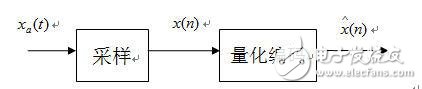
According to the working principle, the spectrum analyzer can be roughly divided into two types: analog and digital. The design is a digital spectrum analyzer. The analyzer first filters the collected signal through a low-pass filter, and then The filtered analog signal is sampled and quantized, amplified by an amplifier and sent to the Atlys Spartan@-6 FPGA Development Kit for digital signal processing, and the spectrum of the signal is obtained by fast Fourier transform.
Demonstration program:
1, FFT principle:
The Fourier transform is a kind of transformation relationship between the time domain description of the signal and the description of the frequency domain. For a certain analog aperiodic signal, there is the following Fourier transform pair
 (1)
(1)
 (2)
(2)
Equation (2) is called the inverse Fourier transform. Equation (1) is called Fourier transform, that is, a function ![]() Yes
Yes ![]() Fourier transform or Fourier integral, function
Fourier transform or Fourier integral, function ![]() Reflecting non-periodic signals
Reflecting non-periodic signals ![]() Spectrum.
Spectrum.
The Fourier transform of a signal is essentially the decomposition of the signal into the sum of sine waves of many different frequencies. The various frequency components of the signal can be obtained by Fourier transform to obtain the spectrum of the signal.
Equation (1) is for the frequency domain, it can be seen as a function of time ![]() The representation on the frequency domain, the information contained in the frequency domain and the information contained in the time domain are identical, the only difference is the form. usually,
The representation on the frequency domain, the information contained in the frequency domain and the information contained in the time domain are identical, the only difference is the form. usually, ![]() Is a complex function, namely:
Is a complex function, namely:
![]() (3)
(3)
![]() with
with ![]() The real and imaginary parts, respectively, the amplitude spectrum (the so-called spectrum)
The real and imaginary parts, respectively, the amplitude spectrum (the so-called spectrum) ![]() Expressed as
Expressed as
![]() (4)
(4)
Therefore, the amplitude spectrum of the spectrum analyzer (that is, the so-called spectrum) can be obtained by the equation (4).
Phase function ![]() Expressed as
Expressed as
 (5)
(5)
This formula reflects the phase frequency characteristics of the signal. The FFT processing module used in this design is the Atlys Spartan®-6 FPGA Development Kit from xilinx, a next-generation Xilinx FPGA learning board that is not only suitable for traditional areas such as VHDL and Verilog HDL code. It can also be used in the next generation of SOPC field learning. The development board is based on the Spartan-6 series XC6SLX9-TQ144 chip. The power supply, download and debugging are completed by the board's own USB interface. The LED, GPIO, UART and USB-JTAG circuits are expanded. The structure is shown in Figure 2. In addition, S6 CARD completes the power supply and debugging of the board through the USB cable, which is convenient to use. The board structure diagram is as follows:
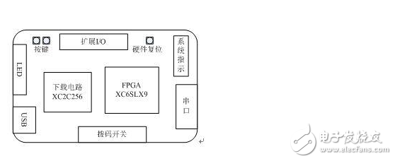
Its main peripherals are listed below:
Xilinx XC6SLX9-TQG144 FPGA;
Comes with USB debugging and power supply circuit (no need to download line and power), CY7C68013, XC2C256;
32M SPI FLASH M25P32;
MAX3232 serial port;
50MHz crystal oscillator;
Button, LED, dial switch
2, the filter principle
The system picks up the signal from the sensor, and often includes a lot of noise and other signals that are not related to the measurement. Therefore, a filter with frequency selection is added to the previous circuit to collect the signal. Filtering is performed.
Filters can be divided into two major categories, analog and digital, depending on the form of the signal being processed. In addition, the three frequency bands of the filter are distributed in different frequency bands, which can select different frequency signals. According to this, the filter can be divided into four different basic types: low-pass filter, high-pass filter, and band. Pass filter, band stop filter. In addition, according to the components used in the filter, it can be divided into: LC passive filter, filter composed of special components, RC passive filter, RC active filter.
In this design, the signal to be acquired is the frequency of 50HZ in the alternating current, and the signal to be collected is directly filtered, so the selected filter is an analog low-pass filter, and if the energy amplification is introduced in the circuit Active devices, such as tubes, transistors, operational amplifiers, etc., complement the lost energy, allowing RC networks to achieve good frequency selection characteristics like LC networks. So the final selected filter is an analog low-pass RC active filter.
The basic form of the analog filter circuit is the current four-segment network, and its characteristics can be expressed as follows:
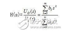
Defined as the ratio of the output to the Laplacian variation of the input signal voltage (or current). In this formula, s=σ+jω is a Laplace variable, and each coefficient ![]() It is a constant determined by the network structure and component parameter values. According to the requirements of the current network stability analysis conditions, each coefficient in the denominator should be positive, and requires n ≥ m, n is called the network order, that is, the order of the filter, the complexity of the reaction circuit.
It is a constant determined by the network structure and component parameter values. According to the requirements of the current network stability analysis conditions, each coefficient in the denominator should be positive, and requires n ≥ m, n is called the network order, that is, the order of the filter, the complexity of the reaction circuit.
In the transfer function, let the Laplace variable s = jω, the frequency characteristic function H(jω) can be obtained:
H(jω)=  =
=  ,
,
The frequency characteristic H(jω) is a complex function, its
A(ω)=  The amplitude is called the amplitude-frequency characteristic.
 ![]() =
= ![]() It is called the phase frequency characteristic.
It is called the phase frequency characteristic.
The second order filter is chosen in this design. The general form of the transfer function is:
 ,make
,make ![]() Corresponding to the natural frequency,
Corresponding to the natural frequency,  Corresponding to the passband gain,
  Corresponding to the damping coefficient, the general form of the transfer function is rewritten to the form of the specification
 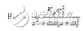 The amplitude-frequency characteristics and phase-frequency characteristics are:
A(ω)= 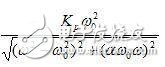
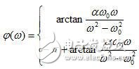
 ,
,
different ![]() The amplitude-frequency characteristics and phase-frequency characteristics of the second-order low-pass filter under the value are as follows:
The amplitude-frequency characteristics and phase-frequency characteristics of the second-order low-pass filter under the value are as follows:
The design platform for the second-order low-pass filter in this design uses the filter design platform provided by Microchip Semiconductor.
3, AD conversion principle:
According to the working principle, it is divided into direct A/D converter and indirect A/D converter. The direct A/D converter converts the analog signal directly into a digital signal. This type of A/D converter has a fast conversion speed. A typical circuit has a parallel comparison type A/D converter and a successive comparison type A/D converter. . The indirect A/D converter converts the analog signal to an intermediate quantity (time or frequency) and then converts the intermediate quantity to a digital output. Such A/D converters are slower, and typical circuits have dual-integration A/D converters and voltage-to-frequency conversion A/D converters. There are many AD conversion chips. According to the needs of the signals collected in this design, the signal is an AC signal, and an 8-bit AD converter is selected. The chip chose the MAX11662 from Maxim. Its parameters are as follows: VDD = 2.2V - 3.6V, VREF = VDD.
The block diagram of the analog-to-digital converter is as follows:
The AD conversion process includes four stages of sampling, holding, quantization, and encoding. By sampling the analog signal at equal intervals T, the sample data on a series of sample points can be obtained, which can be regarded as a time domain discrete signal (sequence). In this design, AD has 8 bits, then each sample data is represented by an 8-bit binary number, that is, a digital signal is formed. Therefore, the process of forming a digital signal after sampling is a process of quantization coding.
4, the principle of the amplifier:
The signal obtained by the low-pass filter may be weak, so the first-stage preamplifier amplifies the acquired signal in order to obtain a signal that is easier to process. There are two purposes for preamplifiers: 1 to make the small input signal not be overwhelmed by the noise of the later circuit; 2 to prevent the noise of the filter circuit from being amplified.
The basic requirements for measuring the amplifier circuit are: 1 the input resistance of the measurement amplifier circuit should match the output impedance of the sensor; 2 stable amplification; 3 low noise; 4 low input offset voltage and input offset current, and low drift; 5 sufficient bandwidth and conversion rate; 6 high common mode input range and high common mode rejection ratio; 7 adjustable closed loop gain; 8 good linearity, high precision; 9 low cost;
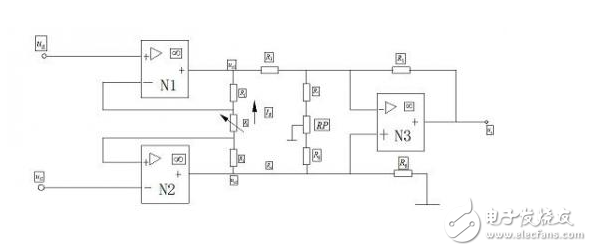
Currently widely used is a high common mode rejection ratio amplification circuit, as shown in the following figure:

The common mode rejection ratio circuit is composed of three integrated operational amplifiers, wherein ![]() A two-phase input universal integrated operational amplifier with consistent performance (mainly input impedance, common mode rejection ratio, and gain) forms a balanced symmetrical (or in-phase parallel) differential amplification input stage.
A two-phase input universal integrated operational amplifier with consistent performance (mainly input impedance, common mode rejection ratio, and gain) forms a balanced symmetrical (or in-phase parallel) differential amplification input stage. ![]() An output stage that forms a single-ended input with a single-ended input for further suppression
An output stage that forms a single-ended input with a single-ended input for further suppression ![]() The common mode signal is adapted to the needs of the grounded load.
The common mode signal is adapted to the needs of the grounded load.
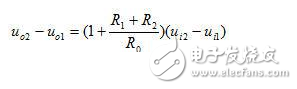
Input stage output voltage, ie operational amplifier ![]() The difference in output is
The difference in output is ![]() Differential mode gain
Differential mode gain
According to the above formula, when 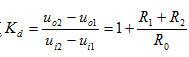 When the performance is consistent, the differential output of the input stage and its differential mode gain are only related to the differential mode input voltage, and its common mode output, offset and drift are both
 ![]() Both ends cancel each other out, so the circuit has good common mode rejection,
Both ends cancel each other out, so the circuit has good common mode rejection, ![]() The bias current is affected, usually
The bias current is affected, usually ![]() .
.
About the amplifier is the LM386, a power amplifier designed for low voltage consumer applications. The internal gain is 20, the input is referenced to ground, and the output is automatically biased to half the supply voltage. With a static power consumption of only 24 milliwatts, the LM386 is ideal for battery operation.
5, LCD output display principle
The LCD has a 7-segment (or 8-segment) display structure, so there are 7 (or 8) segment selection terminals, which must be connected to the segment driver. Each field type of the LCD should be composed of tens of Hz to several hundred Hz. Wave signal drive. The square wave signal is applied to the common electrode of the LCD and the beat signal input of the segment driver. The drive interface circuit of the LCD display is divided into two types of interfaces: static drive and dynamic drive.
The function of the static drive interface is to translate the data to be displayed into a display code through a decoder, and then convert it into a low frequency alternating signal to the LCD display. Dynamic drive interfaces are typically implemented using specialized integrated chips. The main drive and the slave drive are generally used. Both the master and slave drivers use serial data input. The master driver can drive up to 48 display fields or lattices. Each additional slice can drive up to 44 display fields or dot matrix. The driving method uses a 1/3 bias method of 1/4 duty factor.
This design uses a dynamic drive interface serial output.
Wall-mounted UV Air Sterilizer
Uv Sterilizers,Hospital Uv Air Sterilizer,Wall Mounted Uv Air Sterilizer,Wall Mounted Uv Air Sterilizer
Dongguan V1 Environmental Technology Co., Ltd. , https://www.v1airpurifier.com