TCP/IP is a protocol necessary for transmitting data on the Internet. This network communication mode has been improved between PCs, but the size, price and other factors limit the scope of its application. Therefore, the design of network communication based on TCP/IP protocol and Ethernet embedded system has become a hot topic. The system realizes the acquisition of digital TV transport stream (TS) signals and transmission in Ethernet in the embedded system with TI's TMS320DM643 as the core. The system can easily realize the transmission and scheduling of digital TV transmission stream signals in the local area network. The digital television transmission stream source is a digital cable television signal for the European Digital Cable Broadcasting System Standard (DVB-C). The network access hardware is implemented in an embedded system with TMS320DM643 as the core. The network access software is implemented by TI's TCP/IP NDK (Network Developer's Kit) network development kit for the C6000 series DSP.
System circuit design
The circuit is mainly composed of five parts. The block diagram of the digital TV transmission stream network acquisition system is shown in Figure 1. 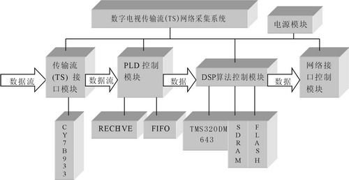
Figure 1 Digital TV transmission stream network acquisition system block diagram
Its main function is to collect digital TV signal through the transport stream interface module and enter the PLD (Cyclone EP1C6Q240C8) chip. After necessary processing, the signal is sent to the DSP (TMS320DM643) chip for storage and algorithm processing. The necessary configuration of the BCM5221 is performed by the TMS320DM643, and the data stored in the TMS320DM643 is transmitted to the local area network through the BCM5221, and the data is received by the computer.
Transport stream interface module
The transport stream interface module consists of the CY7B933 input interface chip and its electrical interface circuit. The CY7B933 input interface circuit is a point-to-point transmission module that enables high-speed serial data transmission over fiber, coaxial cable and twisted pair. The input interface complies with the interface standard of DVB-ASI. After receiving the serial bit stream, the input interface synchronously recovers the clock information of the data through the internal PLL clock, and performs serial-to-parallel conversion, decoding, and transmission error detection on the bit stream. This input interface provides the flexibility to convert high-speed point-to-point serial data into parallel data for a wide range of applications, including server, memory and video transmission applications.
PLD control module
In the project, this part of the hardware is selected by Altera's EP1C6Q240C8 chip.
The main function of this module is to implement the interface with the CY7B933 receiver chip, receive data from CY7B933, and cache data. This part of the function is implemented by functional modules written in the VHDL language. There are two main functional modules: RECEIVE and FIFO. The RECEIVE module is mainly responsible for receiving data fields from CY7B933; the FIFO module is mainly responsible for buffering data.
RECEIVE module
The function of the RECEIVE module is to interface with the CY7B933 receiver chip to receive data from the CY7B933. It works by receiving data on the basis of a transport stream packet.
First, the RECEIVE module detects the boundary of the transport stream packet and determines the number of bytes between the header bytes (fixed to 0x47). Because the data in the packet may also contain 0x47, it is necessary to sacrifice 3 packets of data to check 3 times. When the 0x47 byte is found, an internal counter is triggered to start counting. After counting 188, if the next byte is 0x47, indicating that the transport stream packet belongs to the 188-byte packet, the counter is cleared. If the next byte is 0x47, the transport stream packet belongs to 188 words. The packet is cleared, then the counter is cleared, otherwise the counter is cleared and the boundary is restarted.
When the boundary is detected, the RECEIVE module starts receiving packets. The counter will count from zero, enabling wrreq to output a valid signal while receiving data, and output the data to the next stage. When counting to 188, it indicates that a packet reception is completed. When the data of a packet is received, the counter is cleared, and ts188 is set and held high for one clock cycle. The next cycle detects if the data is 0x47. If it is, it indicates the boundary of the next packet; otherwise, it indicates that an error has occurred and returns to the state of detecting the packet boundary mentioned in the previous paragraph.
In addition, there will be a dedicated counter in the PLD module to record the number of empty packets. When receiving the data packet, it will first detect whether the data packet is empty. If it is an empty packet, the PLD module will delete the empty packet and the counter. Add 1 to China. If the received packet is not empty, the value of the counter is added to the private field of the packet and buffered into the FIFO. The counter is then automatically cleared. The purpose of processing the data packet in this way is to reduce the data traffic transmitted by the network, so that more transport stream data can be transmitted. Adding the value of the counter to the private field is to restore the original empty packet after the computer receives the data, thus ensuring the integrity of the original transport stream data.
FIFO module
The function of the FIFO module is to receive data from the RECEIVE module and cache it. When the RECEIVE module receives a complete transport stream packet, it will send an interrupt signal of ts188 or ts204 to the DSP, and the DSP will start the EDMA function to receive data from the FIFO module. The DSP and FIFO modules are connected asynchronously, and the specific receiving operations are described in the DSP section.
DSP algorithm processing module
This module is mainly composed of embedded system with TMS320DM643 as the core. It mainly implements receiving transport stream data packets from the PLD module, packs the data packets into a TCP/IP format, and implements initialization of the network interface (BCM5221) control module, and then transmits the data packets to the network module.
In order to achieve the above functions, a basic system with TMS320DM643 as the core must be established.
System specific configuration
Clock Configuration: The EMIF core clock ECLKIN is 133MHz. In addition, the system's peripheral bus, EDMA transfer and L2 memory work clock is 1/2 of the CPU core clock, that is, 300MHz; the on-chip timer's working clock is 1/8 of the CPU core clock, that is, 75MHz.
Interrupt Configuration: In addition to the external non-maskable interrupt request input on the RESET and NMI pins, the TMS320DM643 has two external interrupt pins, GP0[5]/EXT_INT5, GP0[7]/EXT_INT7, to provide a maskable external interrupt request input. . In the system, the EXT_INT5 external interrupt is used as the request receiving data signal of the PLD module. When the PLD module receives a transport stream packet, it sends an external interrupt signal to the DSP to inform the DSP to receive the data. In addition, the EDMA interrupt is used to receive the data of a packet for subsequent processing.
System usage of EMIF:
The system expands 4M x 64bit SDRAM memory (MT48LC4M32BPG) in CE0 space for storing programs and data. The operating clock of the SDRAM is provided by the ECLKOUT1 of the TMS320DM643, which is the same as the operating clock frequency of the EMIF. In this system, the default ECLKIN is its clock source, which is 133MHz.
The system expands the 4M x 8bit flash memory (Am29LV033C) in the CE1 space. Before the read/write access to the Flash, the CE1 space of the EMIF control register CE1CTL is required to configure the CE1 space as an 8-bit asynchronous memory interface and read/write timing.
The system expands the interface to the FIFO module in the CE2 space. From the DSP's point of view, the FIFO module can be viewed as an 8-bit asynchronous read-only memory. The read enable signal rdreq of the FIFO module is connected to the CE2 chip select signal of the TMS320DM643; the read clock signal rdclk of the FIFO module is connected to the ARE read enable signal of the TMS320DM643.
Ethernet interface
The TMS320DM643 integrates an EMAC+MDIO on-chip peripheral. EMAC is the abbreviation of Ethernet Media Access Controller, which is the Ethernet media access controller. MDIO is the abbreviation of Management Data Input/Output, which is the management data input/output module. EMAC+MDIO is used to provide an interface to Ethernet physical layer (PHY) devices, where EMAC provides a data path for the interface Ethernet PHY and MDIO provides a management information path for the interface Ethernet PHY.
The block diagram of the TMS320DM643 network interface is shown in Figure 2. Figure 2 depicts an EMAC control module between EMAC+MDIO and DSP. It mainly contains some necessary logic to make EMAC use DSP more effectively, and control some logic of reset and interrupt.
The address space of these registers is: 0x1C800000~0x1C803FFF. 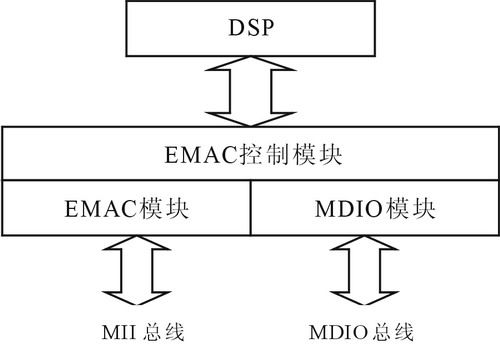
Figure 2 TMS320DM643 network interface block diagram
Network interface control module
This system uses Broadcom's BCM5221 as the 10/100Base-TX Ethernet transceiver. The MII interface of the BCM5221 is connected to the MII interface of the TMS320DM643. The specific interface is shown in Figure 3. The RJ45 connector uses AMP's 406549-1 with two LED indicators on it and the right LED is green to indicate the connection status. The yellow color on the left is used to indicate data transmission under normal conditions. 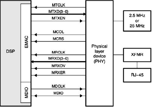
Figure 3 TMS320DM643 and PHY device connection block diagram
Power module
The system includes 4 sets of power supply: the external power supply of the system converts the 220V AC power supply voltage into 5V DC voltage; the PLD module power supply is powered by two power supplies, 3.3V and 1.5V respectively; the TMS320DM643 requires two power supplies, respectively CPU Power is supplied to the core and peripheral I/O interfaces. The peripheral I/O voltage requires 3.3V, the CPU core voltage is only 1.4V, and the network interface control module is powered by a 3.3V power supply.
System software design
The software design of the system is mainly realized by the TCP/IP network development kit NDK. The development kit supports the TCP/IP protocol and consumes less system resources. NDK supports regular TCP/IP services with only 200kB~250kB of program space and 95kB of data space. Therefore, NDK is very suitable for the hardware environment of embedded systems, and is an important tool for DSP network development.
The block diagram of the system software is shown in Figure 4. 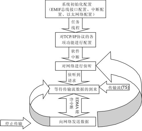
Figure 4 software system diagram
The specific process: the system configuration is mainly done in the initialization function, this initialization function will be called after the .cinit is initialized and before the DSP/BIOS initialization and main function. The system configuration needs to enable the INT8 interrupt, that is, the EDMA transfer interrupt, and set the GPIO7 pin high, so that the PLD module is always in the initial state. The TCP/IP protocol configuration is completed in the task thread, mainly implementing the configuration of the server IP address and gateway. When it is done, the system triggers a software interrupt. In the software interrupt routine, the server generates a port for listening and starts listening for requests on the network. At this point, the server is already on standby, waiting for the client's transfer request.
When the client's transfer request arrives, the system first turns the GPIO7 pin low and the PLD module begins transmitting data. When it receives a complete transport stream packet, it sends an interrupt to the DSP. The DSP starts EDMA and receives the data into a specific memory by ping-pong. After receiving a complete transport stream packet, A hardware EDMA interrupt will be generated. The interrupt program mainly sets the specific flag bit to 1, then exits the hardware interrupt and returns to the software interrupt routine. When the software interrupt routine detects that a particular flag bit is 1, it begins transmitting the transport stream packets in memory to the client. When a packet is transmitted, the specific flag is set to 0 and the system waits for the next packet to arrive.
When the client requests a request to stop transmission, the system will reset the GPIO pin high and the PLD module will return to the initial test state. At this point, the system will be on standby and continue to listen to the network.
system initialization
The initial configuration mainly includes three parts: EMIF bus configuration, interrupt configuration and underlying network configuration. The initialization work is first set in the DSP/BIOS global parameter configuration window, and then the initialization function is called for configuration.
In the DSP/BIOS global configuration window, the working clock frequency of the DSP is set to 600MHz. The chip-level support library CSL selected for use is the DM643 library. The small-end access mode is selected. The 256kB SRAM on the chip is used for Cache and is called. Initialize the function dm643_init().
TCP/IP protocol configuration
After the initialization program dm643_init() is completed, the system will enter each thread. First, the system will trigger the task thread TSK0, execute the function StackTest() in the TSK0 task thread, first call the NC-SystemOpen() function, complete the initialization of the protocol stack and its required memory, and then create a new system configuration handle hCfg = CfgNew ();, and implement the configuration of the server IP address and gateway. In this system, the IP address is configured as "192.168.0.2"; the subnet mask is "255.255.255.0"; the gateway address is "192.168.0.1". Once configured, the system triggers a software interrupt and is ready to listen to the network.
Network listening
In the previous task, the IP address and gateway have been configured. In the following, the port is set and listened in the software interrupt. First, you must assign a file environment fdOpenSession( TaskSelf() ) to this report before you start using the report. Then you can create a report object stcp = socket (AF_INET, SOCK_STREAM, IPPROTO_TCP), and set the port sin1.sin_port = htons (1000), set the port number here to 1000, of course, you can also set other port numbers. Then bind the port number to the report object bind(stcp, (PSA) &sin1, sizeof(sin1). Finally enter the listening state listen (stcp, 1).
Data reception
When the client requests a signal to transmit data, the system will make the GPIO7 pin low and the PLD module will start transmitting data. The DSP receives data by EDMA. EDMA can complete data movement in the DSP memory space by the EDMA controller without CPU involvement. The system mainly uses EDMA's ping-pong method to continuously receive data. The purpose of the ping-pong method is to separate the receiving operation from the sending operation, and to enhance the operability and readability of the program.
Due to space limitations, the network transmission part will not go into details.
Conclusion
The hardware and software functions of this system have been implemented, and the network transmission speed is 2MBps. According to this speed, assuming that the percentage of empty packets in the transport stream is 40%, 5 MBps of transport stream data can be transmitted, and at least 2 to 3 channels of TS stream programs can be transmitted. Therefore, it can be proved that the design method of the system is reasonable and effective.
This article refers to the address: http://
USB Cable advantage:
Made of high quality material(Cable jacket: nylon cloth/fabric/woven/fiber knitt And TPE ,inside:copper wire)with Aluminum Metal shell connectors,Very durable and abrasion resistant,High speed data transfer,Flat cable design is more durable in use,With CE & RoHs certification.
Usb Cable,Usb Data Cables,Data Cable,Usb Mobile Phone Cables
Dongguan City Leya Electronic Technology Co. Ltd , http://www.dgleya.com