1 Introduction
The ADS58H40 is a four-channel, 11/14-bit, 250-MHz, high-performance, high-speed analog-to-digital converter that accepts 90MHz bandwidth from Texas Instruments. It has both a 125MHz bandwidth Burst Mode for feedback and a 90MHz bandwidth SNRBoost Mode for reception, suitable for base station transceiver feedback and receive channels.
Most high-speed analog-to-digital converters (ADCs) currently used in base transceiver stations have a DC offset correction function (DC offset correcTIon funcTIon). It is used to correct the DC received by the ADC so that it does not degrade the performance of the receiver. However, this function also causes code cross-talk of the ADC. If the PCB layout is improper, it will cause the ADC to collect small signal power inaccurately. Taking ADS58H40 as an example, this paper analyzes the problems caused by code domain flipping interference and provides a PCB optimization solution.
2. The role and influence of high-speed ADC DC offset correction function
The DC offset is formed by the DC superposition of the external DC signal component and the original signal. In a base transceiver station, it is mainly caused by the leakage of the local oscillator and the nonlinearity of the mixer or IQ demodulator. The DC offset can interfere with the wanted signal and usually needs to be suppressed using the DC offset correction function of the ADC.
From the code domain point of view, for an ideal 11-bit ADC, the middle code should be 2^(11-1)=1024. Expressed in two's complement is 0x000. Since the most significant bit of the two's complement represents the sign bit, the corresponding 11 bit data range is from 0x000 to 0x7FF. 0x7FF means -1, corresponding to 1023. In the absence of a useful signal input, ideally, the signal acquired by the 11-bit ADC should be 0x000 in the code domain. But in fact, there are thermal noise and DC offsets that are collected by the ADC. The DC offset in the code domain causes the code obtained by the ADC to be offset upward by 0x000, while the natural fluctuation of the thermal noise signal is also superimposed on the code represented by the DC offset. The ADC's DC offset correcTIon function corrects the code domain error caused by the DC offset and recalibrates it to 0x000.
The workflow of the ADC's DC offset correction function is as follows:
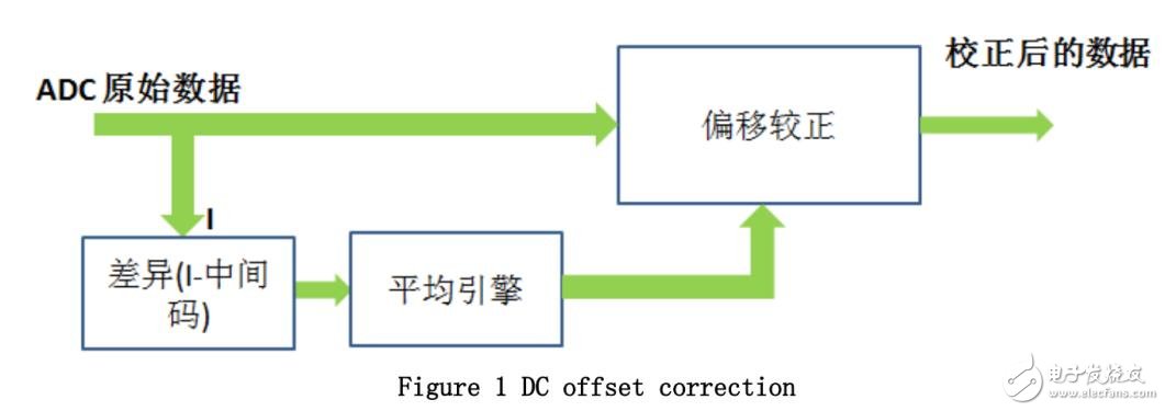
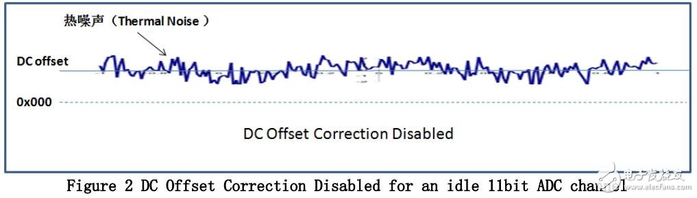
The following two diagrams are used to illustrate the difference between the ADC not enabled and the enabled DC offset correction function in the code domain.
When the DC offset correction function of the ADC is not used, the thermal noise and DC offset obtained by the 11-bit ADC are shown in the code domain as follows:
When using the ADC's DC offset correction function, the thermal noise and DC offset obtained by the 11-bit ADC are shown in the code domain as follows:
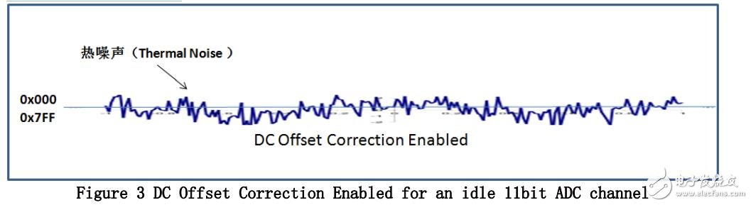
By comparing and finding that the DC offset correction function of the ADC is enabled, the code domain error caused by the DC offset is corrected, and the thermal noise also fluctuates around the DC offset from the basic 0x000 code in the code domain, and becomes around 0x000. Code fluctuations. Therefore, when the DC offset correction function is enabled, natural fluctuations in thermal noise cause random inversions of the code domain from 0x000 to 0x7FF. When the 11 bit data line of the ADC is ADC free, the level of all data lines is switched between logic 0 and logic 1. At this time, the external interference of the data line is the largest. If the PCB layout is not careful enough, this interfering signal is coupled to the analog input of the ADC. Although the amplitude of this coupled interfering signal is not large, it will form a wave-like interference in the frequency domain of the input signal of the ADC, especially the input small signal, and ripple noise (near ripple) when the ADC is airborne. Noise floor).
3, the problem caused by code domain flip interference
Taking the ADS58H40 as an example, the illustration shows the consequences of the code domain flip interference signal coupled to the ADC analog input.
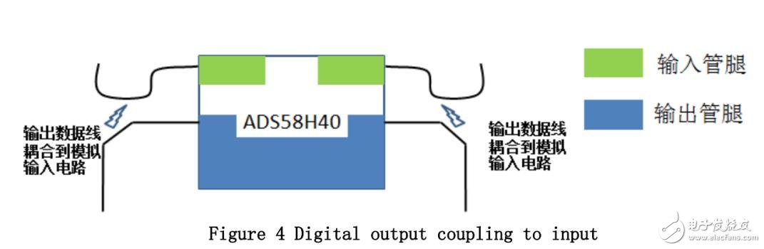
When the PCB layout is not ideal, the output data is directly or indirectly coupled to the analog input of the ADC through the clock or ADC's VCM as shown above.
Affected by the interference signal, the frequency domain diagram obtained by FFT transforming the data obtained by the ADS58H40 channel air sampling is as follows:
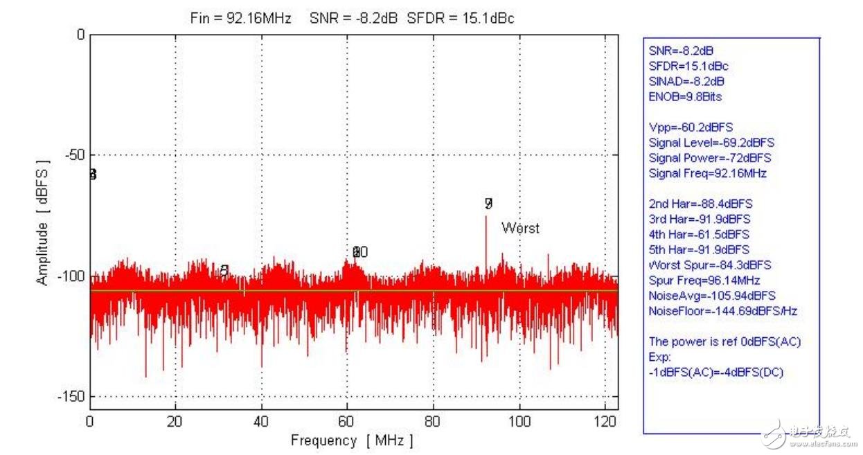
It can be clearly seen from the figure that the ADC collects a wave-type noise floor, which slightly deteriorates the signal-to-noise ratio (SNR) of the ADC, and causes the amplitude measurement of small signals to be inaccurate, which affects the sensitivity of the receiver.
To further illustrate the impact of code domain flipping interference. Use the different amplitude signals to input the ADS58H40 for sweep test. The collected data is plotted as follows:
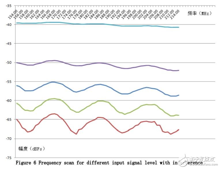
The ADS58H40 has a sampling clock of 245.76 MHz and is swept with 5 power levels for the center 60M range of its second Nyquist domain. When the power is greater than -40dBFs, the code domain flipping interference introduced due to improper PCB layout has little effect on the input signal (the input signal is not completely flat due to the filter relationship at the front end of the ADC). However, as the input signal power decreases, the interference has an increasing influence on the input signal. When the input signal amplitude is lower than -60dBFs, the power error caused by removing the influence of the analog input filter can still reach more than 3dB. .
We are Manufacturer and Supplier to offer Modular Plugs in standard configurations to terminate modular cords for patching or work area applications. Our Modular plugs can be terminated to the exact cable length needed in order to maintain a neater, more organized installation. The modular plugs terminate twisted-pair cable with 26 - 22 AWG (0.40mm - 0.64mm) solid or 7-strand conductors with an insulated conductor diameter of 0.86 - 0.99mm (0.034 - 0.039 in.). All modular plug contacts have 50 microinches minimum of gold plating over nickel and meet TIA-968-A and IEC 60603-7 specifications.
Modular Plug is the name given to a family of electrical connectors originally used in telephone wiring and now used for many other purposes. Many applications that originally used a bulkier, more expensive connector have now migrated to modular connectors. Probably the most well known applications of modular connectors are for telephone jacks and for Ethernet jacks, both of which are nearly always Modular Connectors.
Modular Connectors were originally used with the registered jack system, which precisely describes how the connectors are wired for telecommunications. The registered jack specifications define the wiring patterns of the jacks, not the physical dimensions or geometry of the connectors of either gender. Instead, these latter aspects are covered by ISO standard 8877, first used in ISDN systems. TIA/EIA-568 is a standard for data circuits wired on Modular Plug&Connectors.

Modular Plugs
RJ45 Modular Plugs, RJ11 Modular Plugs, AMP Modular Plugs, Modular Connector, Cat6 Modular Plugs, Cat5e Modular Plugs
NINGBO YULIANG TELECOM MUNICATIONS EQUIPMENT CO.,LTD. , https://www.yltelecom.com